TIDT246 September 2021
4.2 Output Voltage Ripple
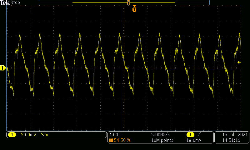
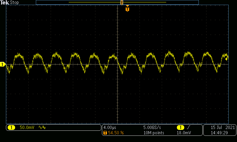
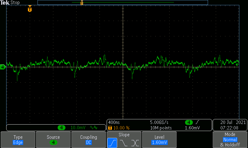
The output voltage ripple of each converter is shown in the following figures.
 Figure 4-9 Boost Converter Output Ripple, 6
VIN, Maximum Load
 Figure 4-10 Boost Converter Output Ripple, 28
VIN, Maximum Load
Figure 4-10 Boost Converter Output Ripple, 28
VIN, Maximum LoadThe LLC output ripple was measured on the 3-W rail to show the worst-case ripple.
 Figure 4-11 LLC Converter Output Ripple, 30
VIN, Maximum Load