TIDT249 September 2021
4.2 CLLLC Waveforms
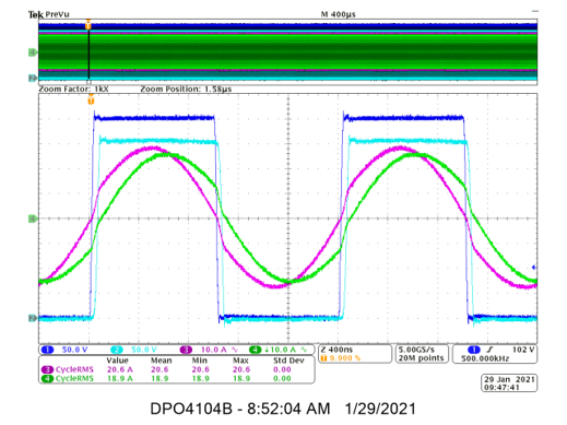
Figure 4-4 shows CLLLC operation at 19 A (6.6 kW) under the following parameters:
- Traces
- C1: GaN Primary Switch Node Drain Voltage
- C2: GaN Secondary Switch Node Drain Voltage
- C3: Transformer Primary Current
- C4: Transformer Secondary Current
- Conditions
- VIN = 400 V
- VOUT = 350 V
- IOUT = 19 A
 Figure 4-4 CLLLC Operation 19 A (6.6
kW)
Figure 4-4 CLLLC Operation 19 A (6.6
kW)Figure 4-5 shows CLLLC operation at 10 A and the following parameters:
- Traces
- C1: GaN Switch Node Drain Voltage Leg 1
- C2: GaN Switch Node Drain Voltage Leg 2
- C3: Transformer Primary Current
- C4: Transformer Secondary Current
- Conditions
- VIN = 400 V
- VOUT = 350 V
- IOUT = 10 A
 Figure 4-5 CLLLC Operation 10 A
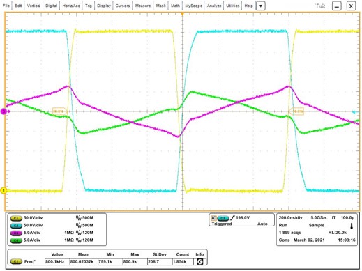
A zoom-in of the GaN switch drain-to-source voltage transition is shown to be approximately 40 ns in Figure 4-6. This rapid transition comes from the low COSS of the LMG3522.
The waveform in Figure 4-6 is measured using the following parameters:
- Traces
- C1: GaN Switch Node Drain Voltage Leg 1
- C2: GaN Switch Node Drain Voltage Leg 2
- C3: Transformer Primary Current
- C4: Transformer Secondary Current
- Conditions
- VIN = 400 V
- VOUT = 350 V
- IOUT = 10 A
 Figure 4-6 CLLLC Operation 10 A - GaN FET
Transitions
Figure 4-6 CLLLC Operation 10 A - GaN FET
TransitionsThe waveform in Figure 4-7 is measured using the following parameters:
- Traces
- C1: GaN Switch Node Drain Voltage Leg 1
- C2: GaN Switch Node Drain Voltage Leg 2
- C3: Transformer Primary Current
- C4: Transformer Secondary Current
- Conditions
- VIN = 400 V
- VOUT = 350 V
- IOUT = 2 A
 Figure 4-7 CLLLC Operation 2 A
A zoom-in of the GaN switch drain-to-source voltage transition is shown to be approximately 75 ns in Figure 4-8. This rapid transition comes from the low COSS of the LMG3522. The slightly longer transition time in this image comes from the lighter load condition and the resulting reduced current flow.
The waveform in Figure 4-8 is measured using the following parameters:
- Traces
- C1: GaN Switch Node Drain Voltage Leg 1
- C2: GaN Switch Node Drain Voltage Leg 2
- C3: Transformer Primary Current
- C4: Transformer Secondary Current
- Conditions
- VIN = 400 V
- VOUT = 350 V
- IOUT = 2 A
 Figure 4-8 CLLLC Operation 2 A - GaN FET
Transitions