TIDT252 December 2021
2.3 Thermal Image
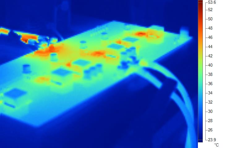
Figure 2-2 shows the thermal image of the top side of the PCB, taken at room temperature, 12.0 VIN and 60.0-A load current.
 Figure 2-2 Thermal Image
TIDT252 December 2021
Figure 2-2 shows the thermal image of the top side of the PCB, taken at room temperature, 12.0 VIN and 60.0-A load current.
 Figure 2-2 Thermal Image