TIDT255 January 2022
3.4 Thermal Images
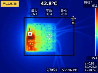
 Figure 3-2 Top layer thermal.
 Vin=24V, 22mA for each rail
Ambient temperature 25℃
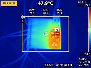
 Figure 3-3 Bottom layer thermal.
 Vin=24V, 22mA for each rail
Ambient temperature 25℃
Highest temperature point: LDO 72.2℃
TIDT255 January 2022
 Figure 3-2 Top layer thermal.
 Vin=24V, 22mA for each rail
Ambient temperature 25℃
 Figure 3-3 Bottom layer thermal.
 Vin=24V, 22mA for each rail
Ambient temperature 25℃
Highest temperature point: LDO 72.2℃