TIDT261 March   2022


  1.   Description
  2.   Features
  3.   Applications
  4. 1Test Prerequisites
    1. 1.1 Voltage and Current Requirements
    2. 1.2 Considerations
    3. 1.3 Dimensions
  5. 2Testing and Results
    1. 2.1 Efficiency Graphs
    2. 2.2 Load Regulation
    3. 2.3 Line Regulation
    4. 2.4 Thermal Images
      1. 2.4.1 4-V Input Voltage
        1. 2.4.1.1 3-A Output Current – Average Load Current
        2. 2.4.1.2 5-A Output Current – Peak Load Current
      2. 2.4.2 12-V Input Voltage
        1. 2.4.2.1 3-A Output Current
        2. 2.4.2.2 5-A Output Current
      3. 2.4.3 18-V Input Voltage
        1. 2.4.3.1 3-A Output Current
        2. 2.4.3.2 5-A Output Current
    5. 2.5 Bode Plots
  6. 3Waveforms
    1. 3.1 Switching
    2. 3.2 Output Voltage Ripple
    3. 3.3 Input Voltage Ripple
    4. 3.4 Load Transients
    5. 3.5 Start-Up Sequence
    6. 3.6 Shutdown Sequence

Output Voltage Ripple

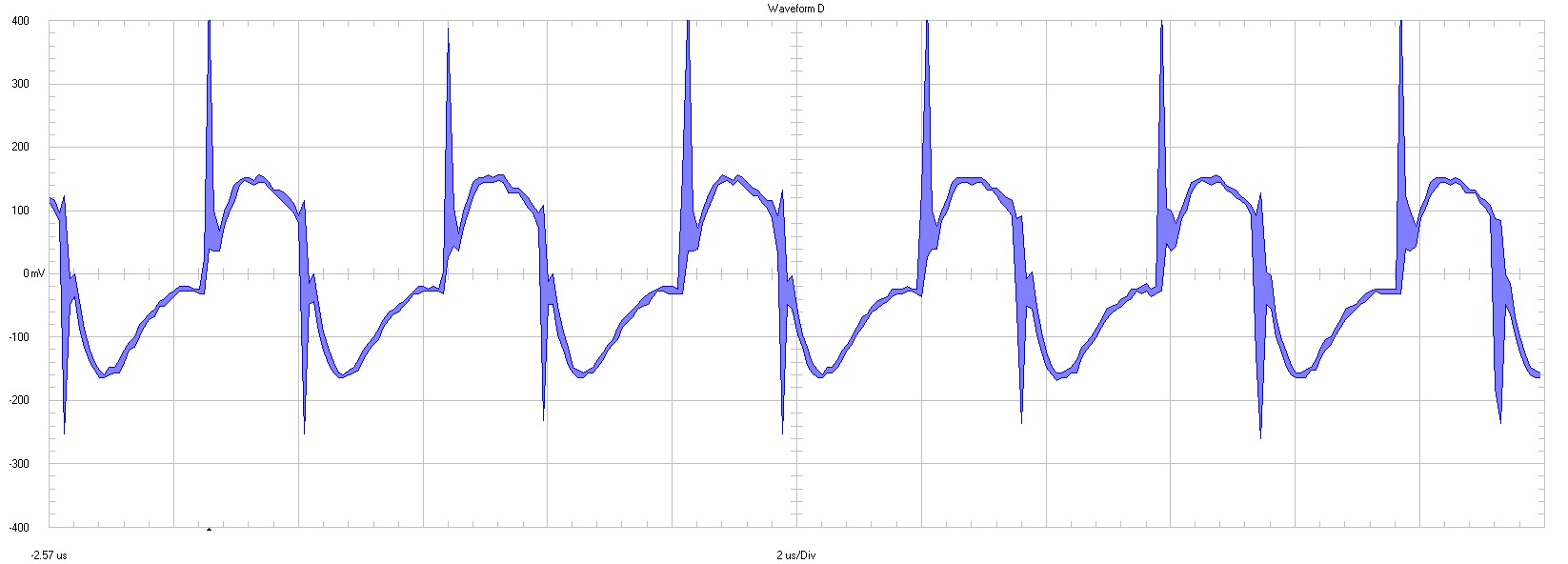
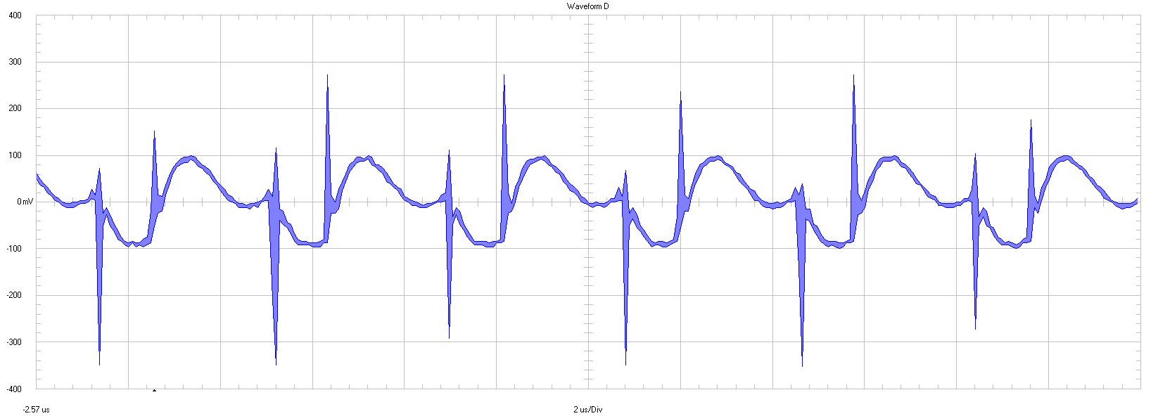
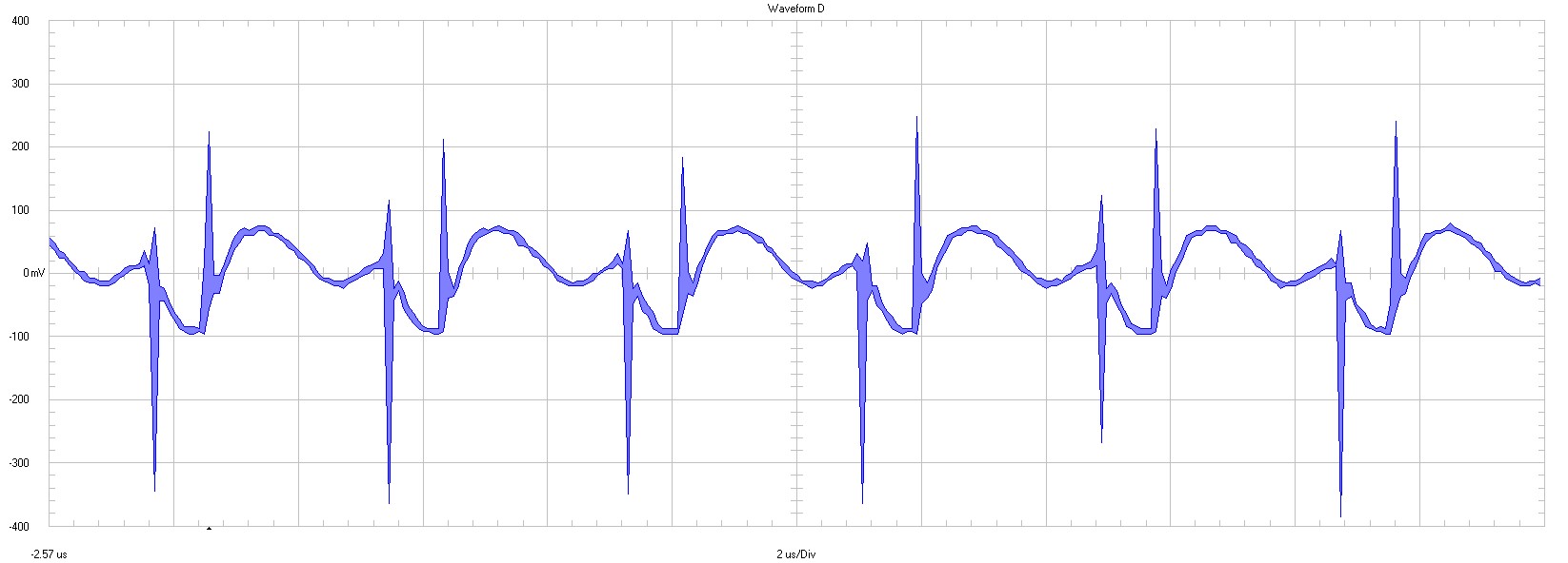
Output voltage ripple (AC coupled) is shown in the following figures.
GUID-20220224-SS0I-LBD1-RTVG-DNLM0WSHPR4W-low.jpg
100 mV / div, 20-MHz bandwidth, 2-µs / div
Figure 3-12 Output Voltage Ripple at 4 VIN
GUID-20220224-SS0I-MNNS-KJFL-KNW4GZM9HS3Q-low.jpg
100 mV / div, 20-MHz bandwidth, 2-µs / div
Figure 3-13 Output Voltage Ripple at 12-VIN
GUID-20220224-SS0I-4JX8-15QZ-RT2FBRN64V8J-low.jpg
100 mV / div, 20-MHz bandwidth, 2-µs / div
Figure 3-14 Output Voltage Ripple at 18-VIN