TIDT262 April 2022
- Description
- Features
- Applications
- 1Test Prerequisites
-
2Testing and
Results
- 2.1 Efficiency Graphs
- 2.2 Load Regulation
- 2.3 Line Regulation
- 2.4
Thermal Images
- 2.4.1
Further Extensive Thermal
Measurements
- 2.4.1.1
No Forced Cooling
- 2.4.1.1.1 Thermal Images 4.5 VIN and 20 AOUT
- 2.4.1.1.2 Thermal Image 5.5 VIN and 20 AOUT
- 2.4.1.1.3 Thermal Image 7 VIN and 25 AOUT
- 2.4.1.1.4 Thermal Image 9 VIN and 30 AOUT
- 2.4.1.1.5 Thermal Image 12 VIN and 30 AOUT
- 2.4.1.1.6 Thermal Image 15 VIN and 30 AOUT
- 2.4.1.1.7 Thermal Image 13.8 VIN and 30 AOUT
- 2.4.1.2 Forced Cooling
- 2.4.1.1
No Forced Cooling
- 2.4.1
Further Extensive Thermal
Measurements
- 2.5 Bode Plots
- 3Waveforms
2.5 Bode Plots
Table 2-1 details a summary of the test results from the bode plots.
Table 2-1 Summary of the Bode Plots Test Results
|
VIN |
4.5 V | 7 V | 9 V | 12 V | 16 V | 27 V |
|
Bandwidth (kHz) |
0.956 |
1.54 |
2.0 |
2.72 |
3.75 |
3.68 |
|
Phase Margin |
61.2° |
73.7° |
78° |
80.9° |
77.4° |
82.2 |
|
Slope (20 dB/decade) |
–1.18 |
–1 |
–1.1 |
–0.77 |
–1.2 |
–1 |
|
Gain Margin (dB) |
–14.8 |
20.2 |
–20.5 |
–18.4 |
25 |
–26.5 |
|
Slope (20 dB/decade) |
–1.3 |
–1.4 |
–1.11 |
–1.41 |
–2.4 |
–2.3 |
|
Freq (kHz) |
5.59 |
23.8 |
–24.9 |
24.4 |
39.7 |
46 |
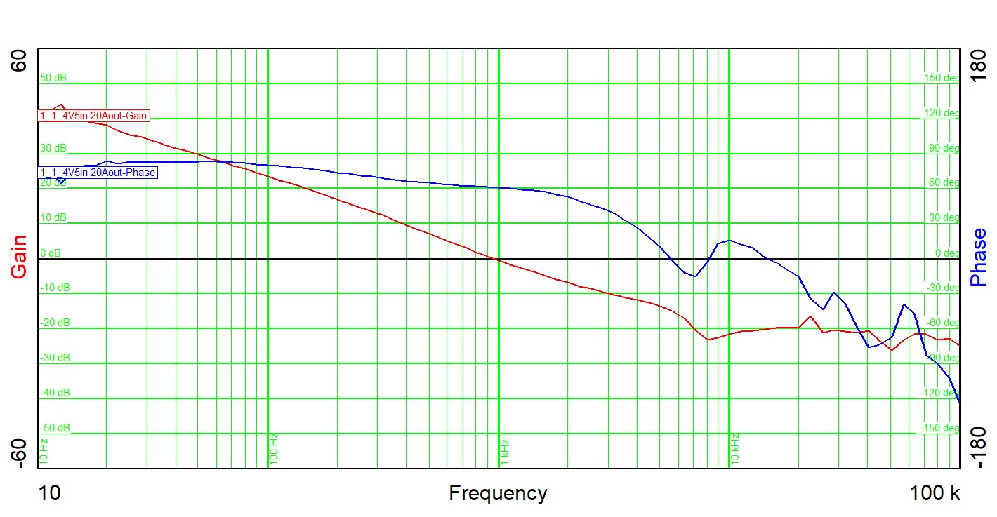 Figure 2-24 Bode Plot for 4.5-V Input
Voltage and 20-A Output Voltage
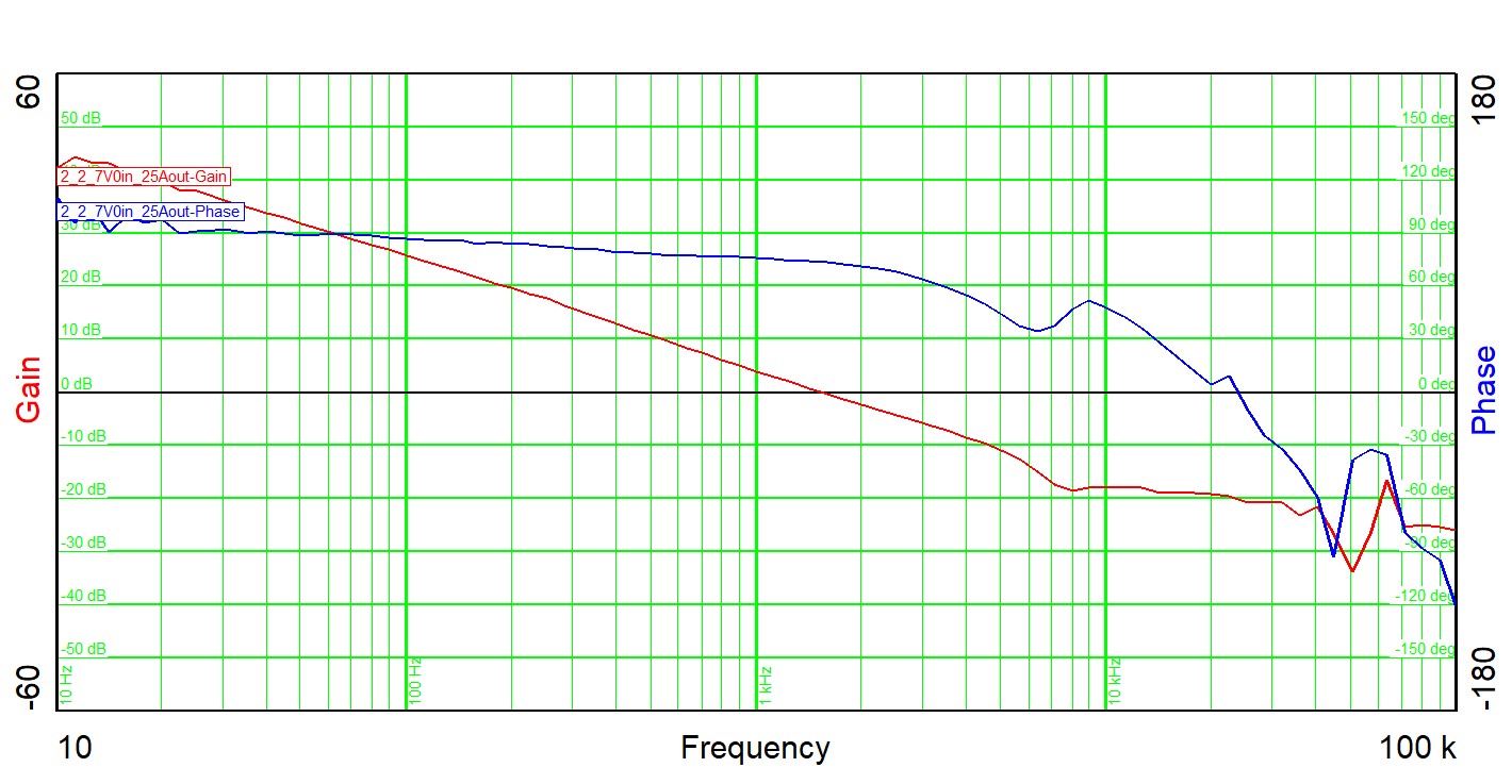 Figure 2-25 Bode Plot for 7-V Input
Voltage and 25-A Output Voltage
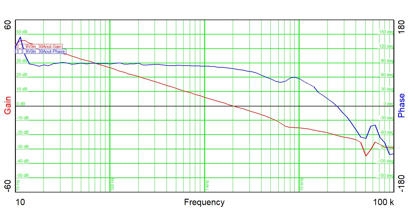 Figure 2-26 Bode Plot for 9-V Input
Voltage and 30-A Output Voltage
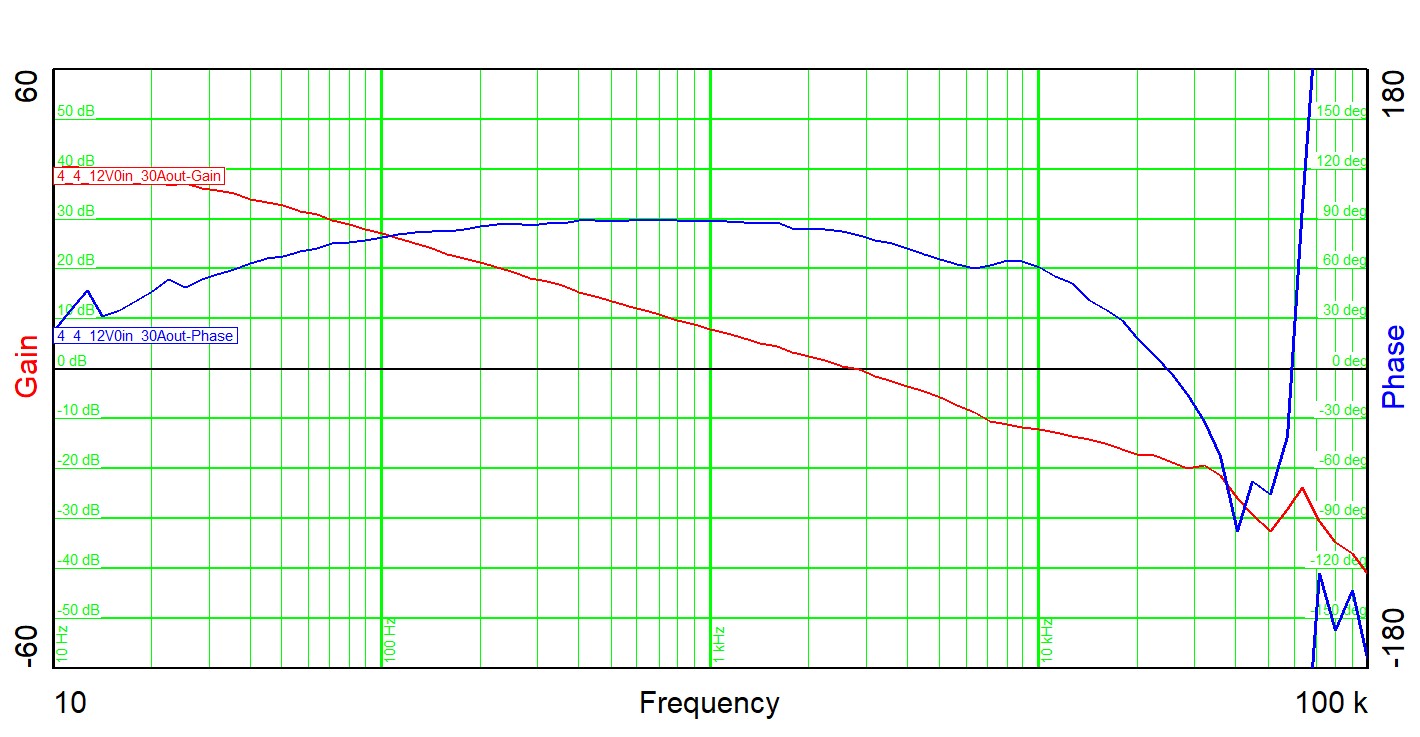 Figure 2-27 Bode Plot for 12-V Input
Voltage and 30-A Output Voltage
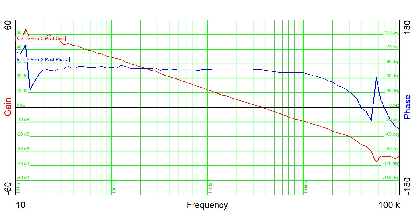 Figure 2-28 Bode Plot for 16-V Input
Voltage and 30-A Output Voltage
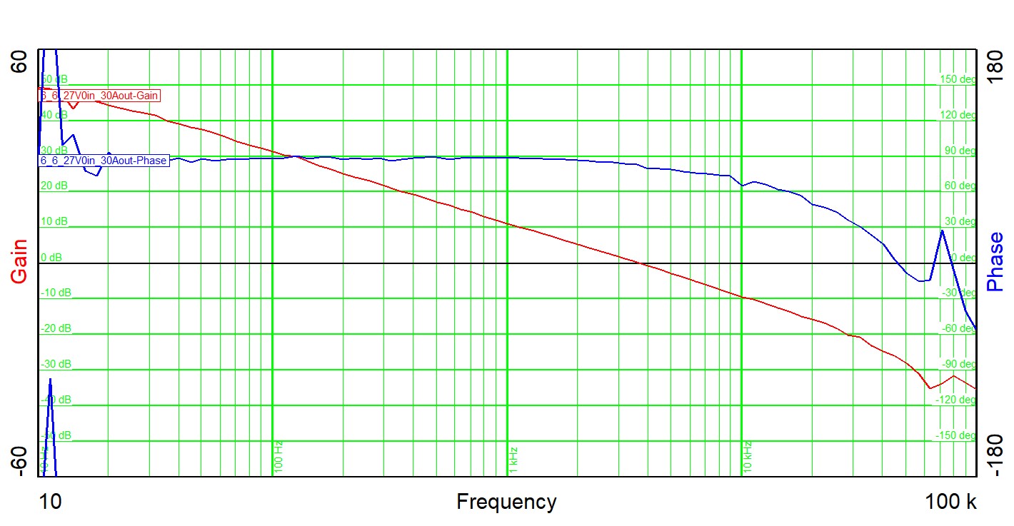 Figure 2-29 Bode Plot for 27-V Input
Voltage and 30-A Output Voltage