TIDT263 March 2022
3.1 Switching
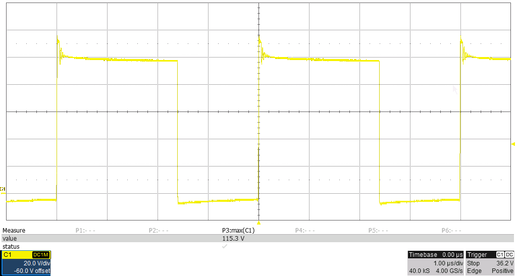
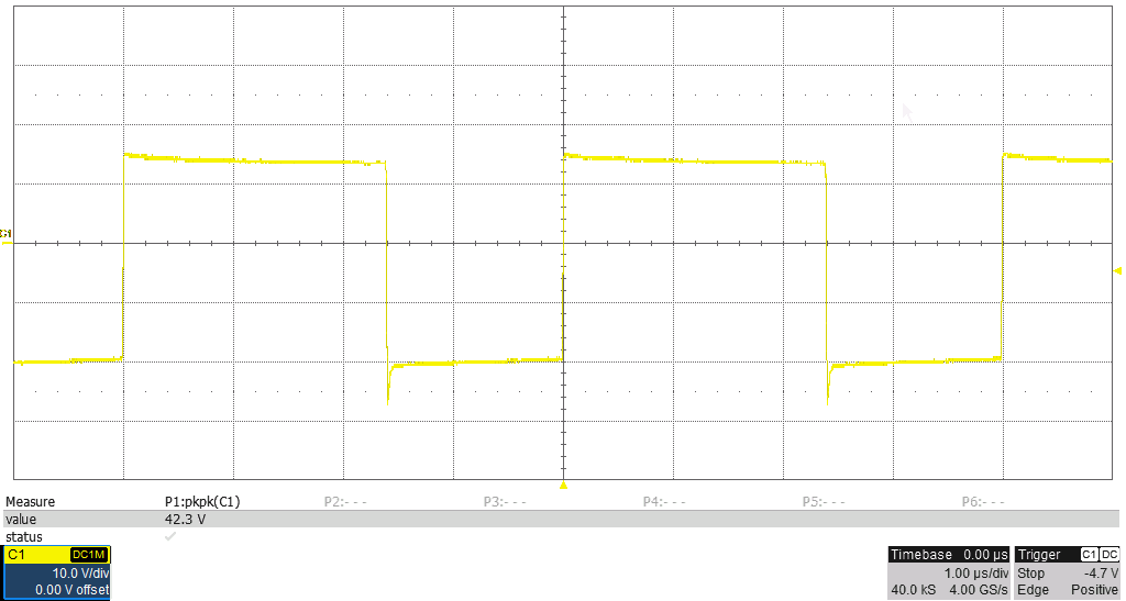
Switching behavior is shown in the following figures.
 Figure 3-1 Voltage Drain to PGND, Q2,
57-V Input, 2.1-A Load, 20 V/div, 1 μs/div, Measured 115.3 Vpeak
 Figure 3-2 Voltage Anode to GND, D100,
57-V Input, 2.1-A Load, 10 V/div, 1 μs/div, Measured 42.3 Vpeak