TIDT269 April 2022
3.1 Switching
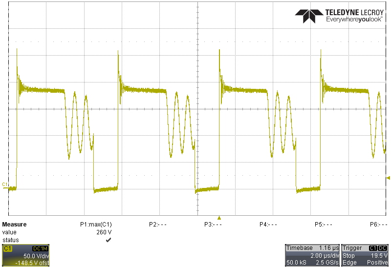
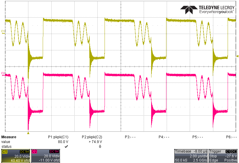
Switching behavior is shown in the following figures.
 Figure 3-1 Vds of Primary FET (Q3),
120-VDC Input, 40-W Output
 Figure 3-2 Voltage on Anodes of Output
Diodes (D1 on Ch1, D2 on Ch2), 120-VDC Input, 20-W Each Output