-
Ultra-Wide Input, 10-W Isolated Flyback Reference Design
TEST REPORT
Ultra-Wide Input, 10-W Isolated Flyback Reference Design
Description
This reference design is a wide-VIN, low-power flyback design that can take dual inputs from 19 VDC to 60 VDC and 85 VAC to 275 VAC. It is designed to provide 24 V at 420 mA to the output load.
Features
- Ultra-wide input
- Small form factor
- Excellent regulation over wide input
Applications
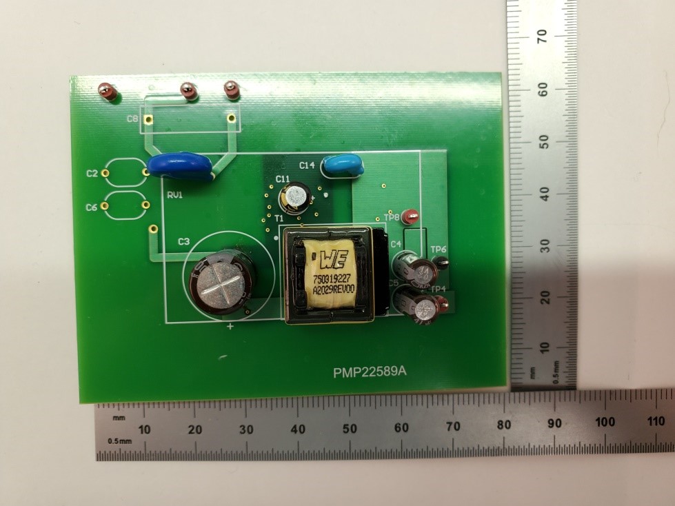
 Board Photo
(Top)
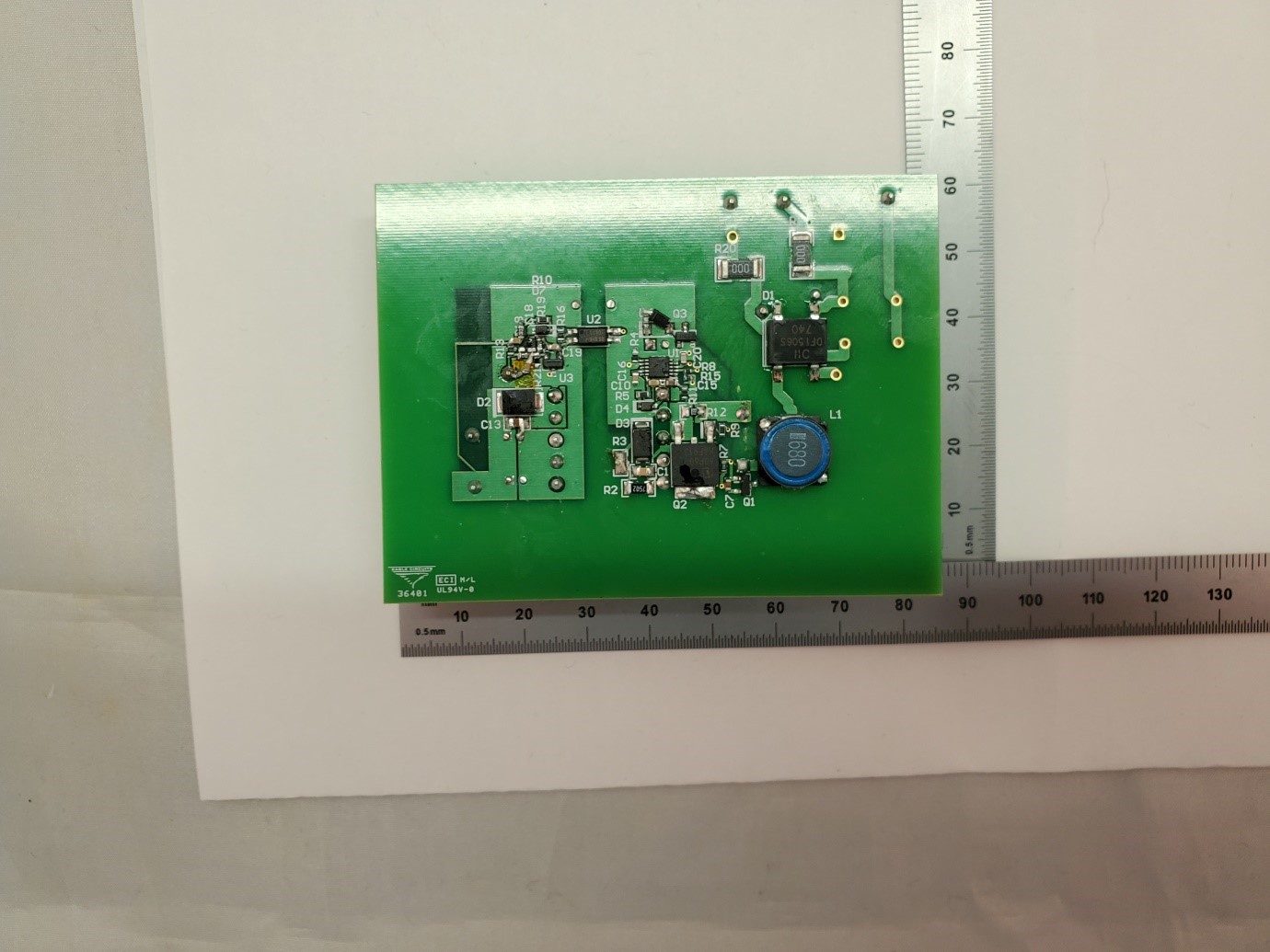
 Board Photo
(Bottom)