TIDT277 April   2022


  1.   Description
  2.   Features
  3.   Applications
  4. 1Test Prerequisites
    1. 1.1 Voltage and Current Requirements
    2. 1.2 Considerations
    3. 1.3 Dimensions
  5. 2Testing and Results
    1. 2.1 Efficiency Graphs, all Outputs Similar Loaded
    2. 2.2 Load Regulation
    3. 2.3 Cross Regulation and Further Data For Non-Symmetrical Loading
    4. 2.4 Line Regulation at Full Load to all Outputs
    5. 2.5 Thermal Images
  6. 3Waveforms
    1. 3.1 Switching
      1. 3.1.1 Switchnode to GND
      2. 3.1.2 Diode D3
    2. 3.2 Output Voltage Ripple
    3. 3.3 Input Voltage Ripple
      1. 3.3.1 Power Stage Input
      2. 3.3.2 Between L1 and L2
      3. 3.3.3 Input Terminal
    4. 3.4 Start-Up Sequence
    5. 3.5 Shutdown Sequence

Between L1 and L2

GUID-20220405-SS0I-NPWP-M5ZZ-TSQMQX9FRNZ0-low.jpg

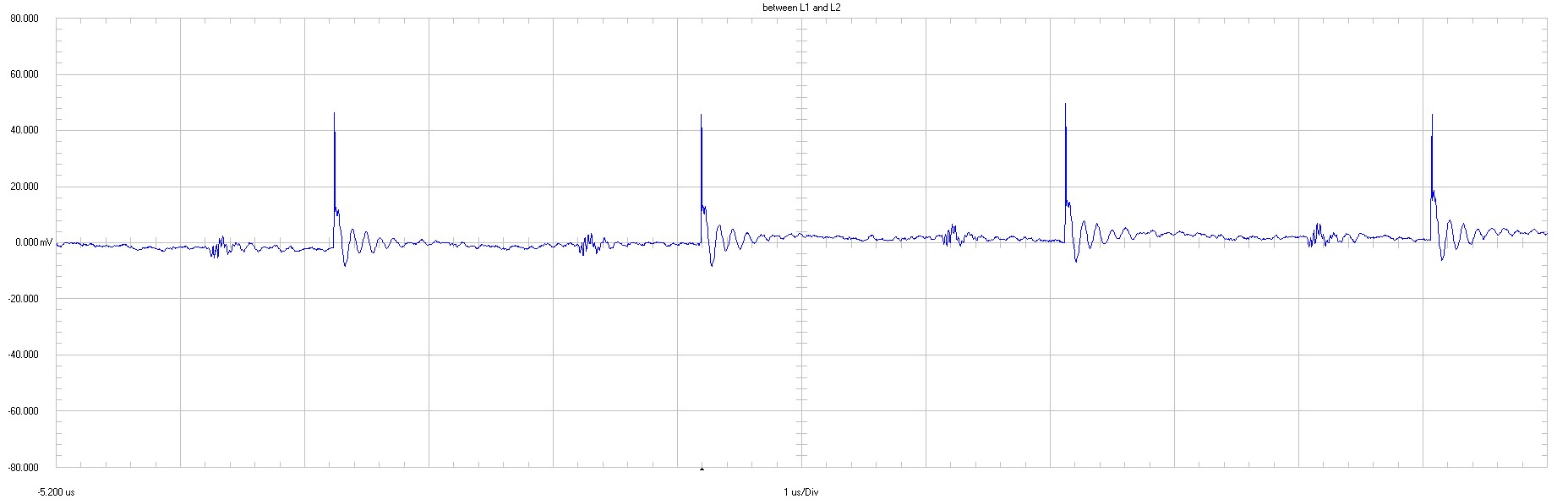
20 mV / div

1 µs / div

20 MHz bandwidth

Figure 3-6 Voltage Ripple Between L1 and L2, Ripple Attenuation by Differential LC Filter