TIDT279 October 2022
3.2 Load Transients
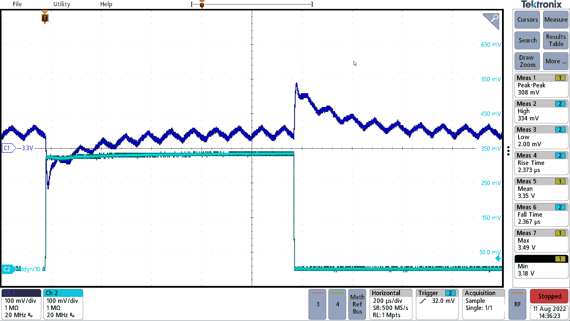
Figure 3-4 shows the load transient waveform at 8 V. The waveform was taken at 14 VIN with the load going from 3 A to 6.35 A and back to 3 A. The onboard dynamic load (J301 and Q300) was driven by Tektronix AFG3102.

Output undershoot and overshoot
each about 150 mV (purple trace). Dynamic current measured at J300 across a
100-mΩ shunt R306 on the PMP23194 board (blue trace).
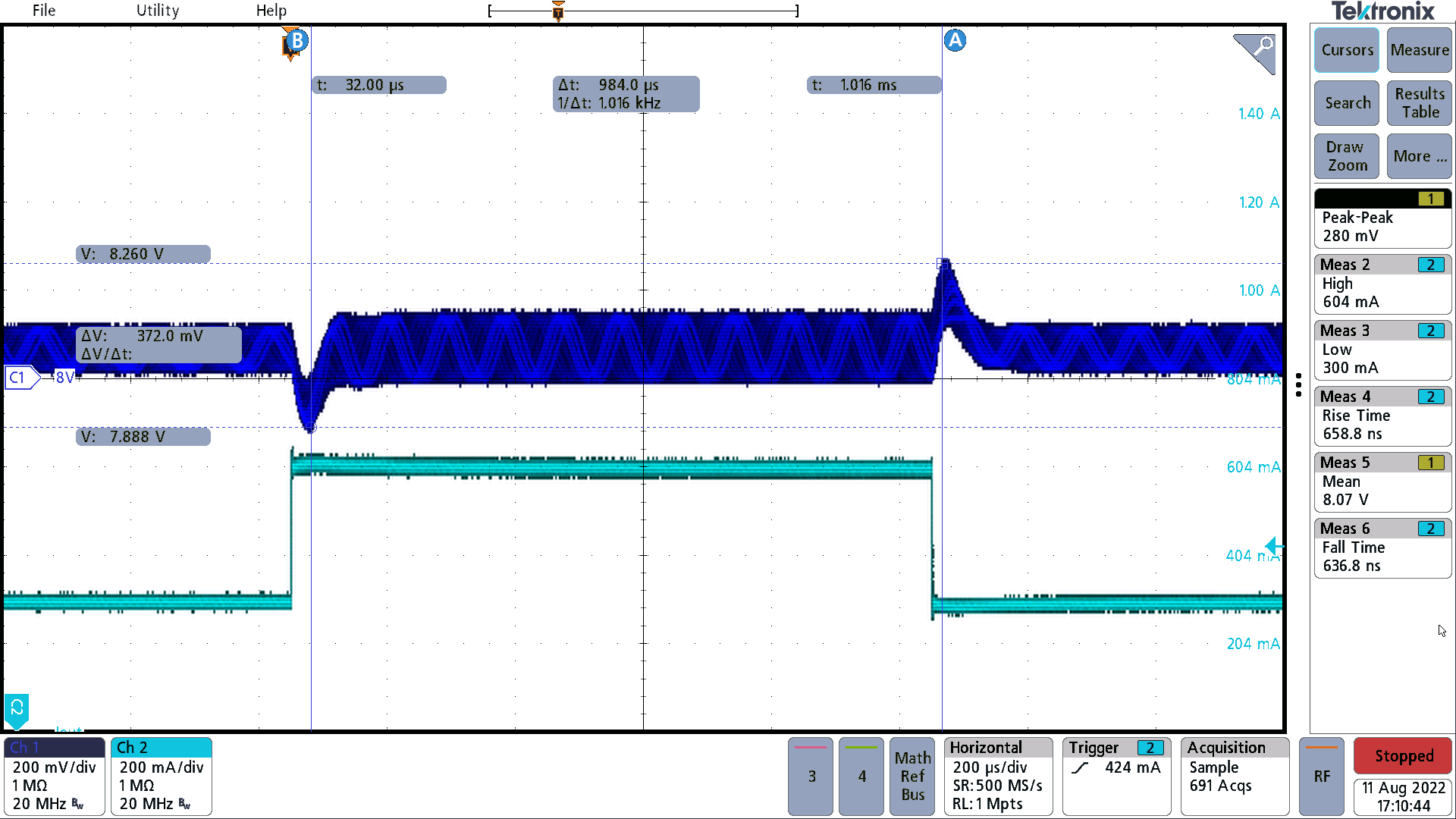
Figure 3-4 Load Transient 3.3 VFigure 3-5 shows the load transient waveform at 8 V. The waveform was taken at 14 VIN with the load going from 300 mA to 600 mA and back to 300 mA. Dynamic load inside the Kikusui PLZ334WA was used.

Undershoot and overshoot are each
about 120 mV (dark blue trace). Dynamic current was measured with clip-on
current probe (blue trace).
Figure 3-5 Load Transient 8 V