TIDT279 October 2022
2.2 Thermal Images
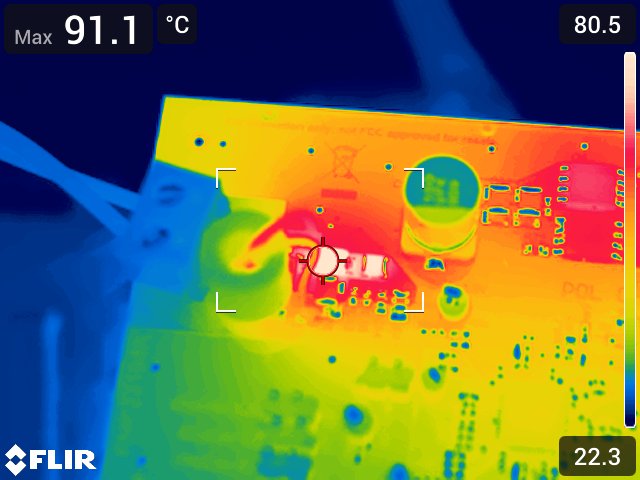
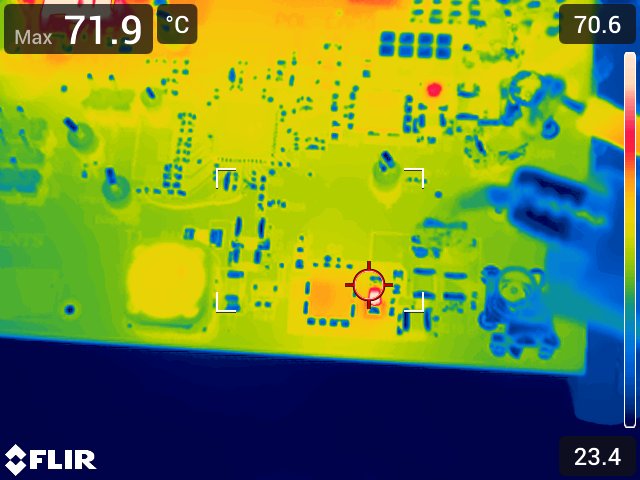
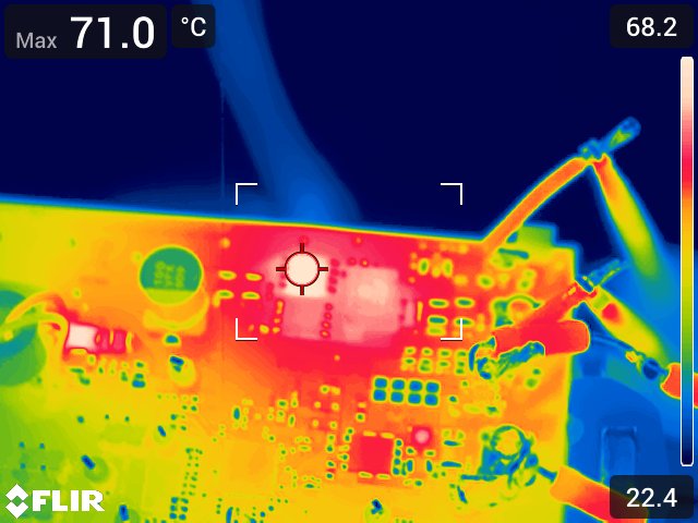
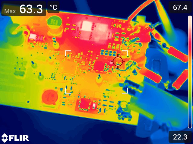
Figure 2-7 through Figure 2-10 show the worst-case thermal images. All outputs are loaded to their maximum; or 6.7 A off the 3.3 V, 120 mA off the 5 V, and 600 mA off the 8 V. Thermal images were taken at 10 VIN, 14 VIN and 18 VIN. Ambient is room temperature or about 22°C, and there are no fans blowing on the boards.
 Figure 2-7 Input Reverse Protection
Diode D1 Worst Case at 10 VIN, 91°C
 Figure 2-9 Output Rectifier of the 8-V SEPIC D2 Worst Case at 10 VIN,
72°C
 Figure 2-8 High-Side FET Q4 of the 3.3-V Buck Converter Worst Case at 18
VIN, 71°C
 Figure 2-10 Main Inductor of the 5-V Buck L2 Worst Case at 18 VIN,
63°C