TIDT279 October 2022
1.1 Power and Load Connections and Test Points
Table 1-1 describes power and load connections. Table 1-2 lists the test point descriptions and devices.
Table 1-1 Power and Load Connections
| Connections | Description |
|---|---|
| J-BAT | VIN to LM5127-Q1 three-output power
supply 9-V to 18-V steady state main power input 2 × 1 5.08-mm terminal block |
| J8 and J8R | 8-V, 600-mA SEPIC output, 2 × Keystone 1212-ST
(0.187 in [4.75 mm] Quick-connect male solder connector non-insulated) |
| J5 and J5R | 5-V, 120-mA buck output, 2 × Keystone 1212-ST |
| J3 and J3R | 3.3-V, 6.7-A buck output, 2 × Keystone 1212-ST |
Table 1-2 Test Points
| Test Point | Description | Device |
|---|---|---|
| SP8 | 8-V output sense | MCX jack receptacle |
| TP801 | Bode plot injection point for the 8-V loop | |
| TP1 | Active low when any output active | |
| J55 | Jumper to disable 5 V | TSW-102-07-G-S |
| J33 | Jumper to disable 3.3 V | TSW-102-07-G-S |
| SP5 | 5-V output sense | MCX jack receptacle |
| TP501 | Bode plot injection point for the 5-V loop | |
| SP3 | 3.3-V output sense | MCX jack receptacle |
| TP301 | Bode plot injection point for the 3.3-V loop | |
| J300 | Dynamic current monitor off the 3.3-V dynamic load | Receptacle, ultra miniature coaxial, male pin, 50-Ω, SMT |
| J301 | Signal generator injection for the 3.3-V dynamic load | TSW-102-07-G-S |
| J302 | Not used, was to change 3.3-V loop speed |
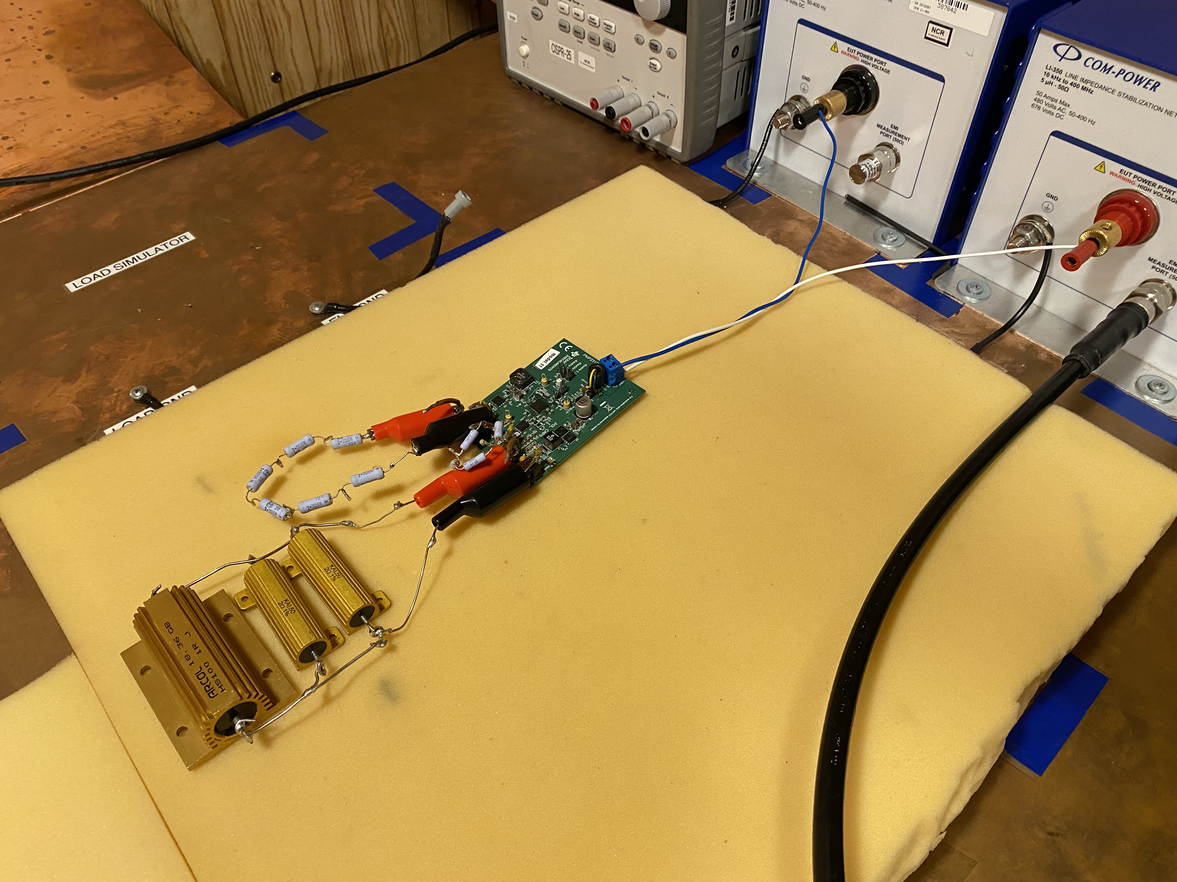
Figure 1-1 shows the test setup.
 Figure 1-1 Test Setup for Conducted Emissions