TIDT281 June   2022


  1.   Description
  2.   Features
  3.   Applications
  4. 1Test Prerequisites
    1. 1.1 Voltage and Current Requirements
    2. 1.2 Considerations
    3. 1.3 Dimensions
  5. 2Testing and Results
    1. 2.1 Efficiency Graphs
      1. 2.1.1 24-V Output Voltage
      2. 2.1.2 48-V Output Voltage
    2. 2.2 Loss Graphs
      1. 2.2.1 24-V Output Voltage
      2. 2.2.2 48-V Output Voltage
    3. 2.3 Load Regulation
      1. 2.3.1 24-V Output Voltage
      2. 2.3.2 48-V Output Voltage
    4. 2.4 Line Regulation
      1. 2.4.1 24-V Output Voltage
      2. 2.4.2 48-V Output Voltage
    5. 2.5 Thermal Images
    6. 2.6 Bode Plots
      1. 2.6.1 60-V Input Voltage and 24-V Output Voltage
      2. 2.6.2 30-V Input Voltage and 48-V Output Voltage
      3. 2.6.3 Loop Variants
  6. 3Waveforms
    1. 3.1 Switching
      1. 3.1.1 24-V Output Voltage, 30-V Input Voltage (Duty Cycle 80%)
        1. 3.1.1.1 Diode D1
        2. 3.1.1.2 Transistor Q2
          1. 3.1.1.2.1 Drain - GND
          2. 3.1.1.2.2 Gate - GND
        3. 3.1.1.3 Diode D2
        4. 3.1.1.4 Transistor Q1
          1. 3.1.1.4.1 Source - VIN
          2. 3.1.1.4.2 Gate - Source
      2. 3.1.2 24-V Output Voltage; 60-V Input Voltage
        1. 3.1.2.1 Diode D2
        2. 3.1.2.2 Transistor Q1
          1. 3.1.2.2.1 Source - VIN
          2. 3.1.2.2.2 Gate-Source
      3. 3.1.3 48-V Output Voltage; 30-V Input Voltage (Maximum Stress)
        1. 3.1.3.1 Diode D1
        2. 3.1.3.2 Transistor Q2
          1. 3.1.3.2.1 Drain-GND
          2. 3.1.3.2.2 Gate-GND
        3. 3.1.3.3 Diode D2
        4. 3.1.3.4 Transistor Q1
          1. 3.1.3.4.1 Source - VIN
          2. 3.1.3.4.2 Gate - Source
      4. 3.1.4 48-V Output Voltage; 60-V Input Voltage
        1. 3.1.4.1 Diode D1
        2. 3.1.4.2 Transistor Q2
          1. 3.1.4.2.1 Drain - GND
          2. 3.1.4.2.2 Gate - GND
        3. 3.1.4.3 Diode D2
        4. 3.1.4.4 Transistor Q1
          1. 3.1.4.4.1 Source - VIN
          2. 3.1.4.4.2 Gate - Source
    2. 3.2 Output Voltage Ripple
      1. 3.2.1 24-V Output Voltage
      2. 3.2.2 48-V Output Voltage
    3. 3.3 Input Voltage Ripple
      1. 3.3.1 24-V Output Voltage
      2. 3.3.2 48-V Output Voltage
    4. 3.4 Load Transients
      1. 3.4.1 24-V Output Voltage
        1. 3.4.1.1 30-V Input Voltage
        2. 3.4.1.2 60-V Input Voltage
      2. 3.4.2 48-V Output Voltage
        1. 3.4.2.1 30-V Input Voltage
        2. 3.4.2.2 60-V Input Voltage
    5. 3.5 Start-Up Sequence
      1. 3.5.1 24-V Output Voltage
        1. 3.5.1.1 30-V Input Voltage
        2. 3.5.1.2 60-V Input Voltage
      2. 3.5.2 48-V Output Voltage
        1. 3.5.2.1 30-V Input Voltage
        2. 3.5.2.2 60-V Input Voltage
    6. 3.6 Shutdown Sequence
      1. 3.6.1 24-V Output Voltage
        1. 3.6.1.1 30-V Input Voltage
        2. 3.6.1.2 60-V Input Voltage
      2. 3.6.2 48-V Output Voltage
        1. 3.6.2.1 30-V Input Voltage
        2. 3.6.2.2 60-V Input Voltage
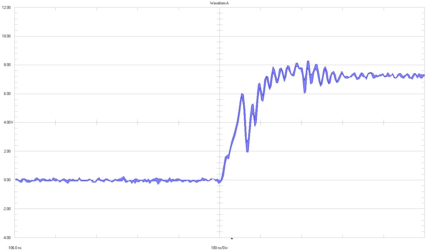
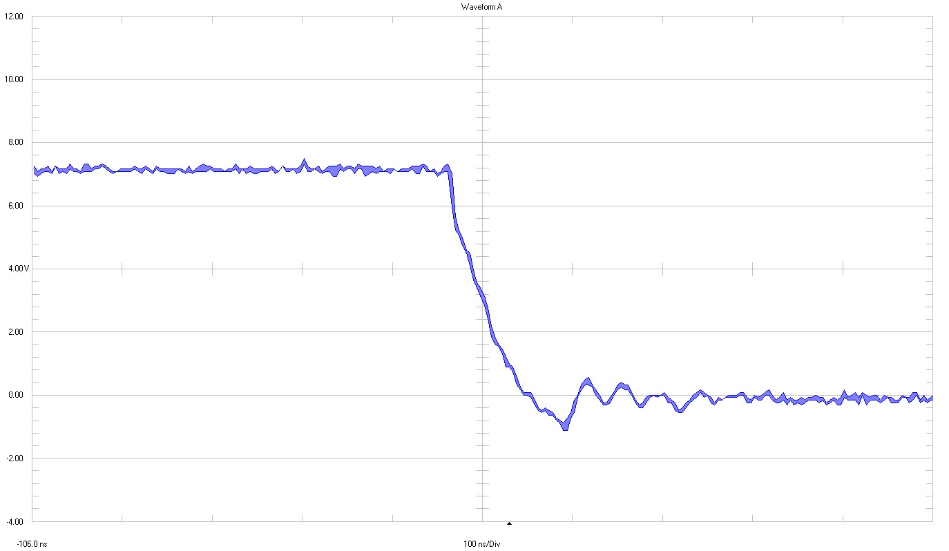
Gate-GND
Note: The final application uses FETs with much lower gate charge QG. A gate resistor (3.3 Ω to 4.7 Ω) might reduce the ringing on the gate.
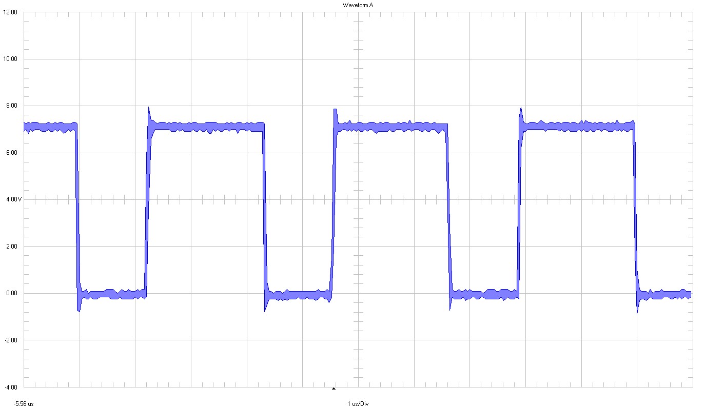
GUID-20220509-SS0I-QQ26-2DW7-RCCFF5G36GQ6-low.jpg

2 V / div

1 µs / div

full bandwidth

GUID-20220509-SS0I-LJJJ-5FJR-F6CSMJVTHTJS-low.jpg
GUID-20220509-SS0I-X1BG-WG94-V9TPPC8VWZ6K-low.jpg

2 V / div

200 ns full scale

full bandwidth

Figure 3-15 Transistor Q2 Gate - GND