TIDT282 May 2022
3.3 Start-Up Sequence
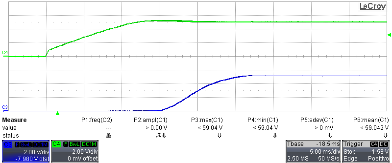
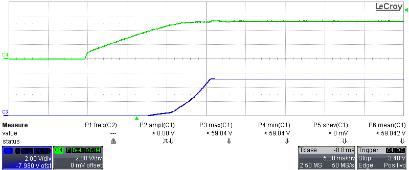
The behavior of the converter, showing VIN and the output voltage, is shown in Figure 3-5 and Figure 3-6. The input voltage has been set to 5 V.

C3: Output Voltage (2 V/div, 5
ms/div, 20-MHz BWL)
C4: Input Voltage (2 V/div, 20-MHz BWL)
IOUT = 750 mA
Figure 3-5 Start-Up With IOUT = 750 mAC4: Input Voltage (2 V/div, 20-MHz BWL)
IOUT = 750 mA

C3: Output Voltage (2 V/div, 5
ms/div, 20-MHz BWL)
C4: Input Voltage (2 V/div, 20-MHz BWL)
IOUT = 0 mA
Figure 3-6 Start-Up With IOUT = 0 AC4: Input Voltage (2 V/div, 20-MHz BWL)
IOUT = 0 mA