TIDT282 May 2022
3.1 Switching
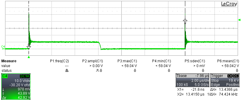
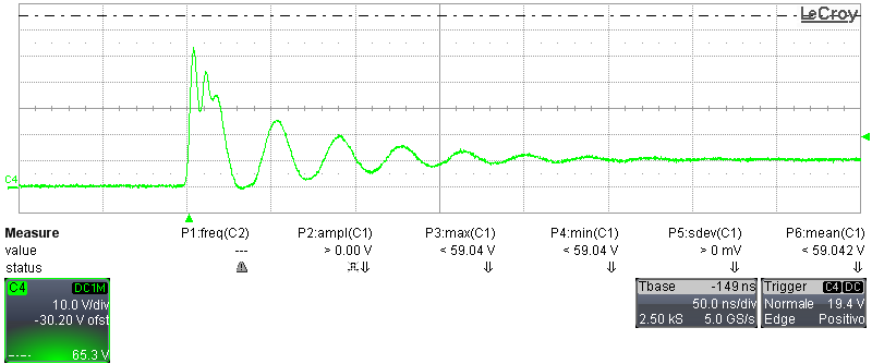
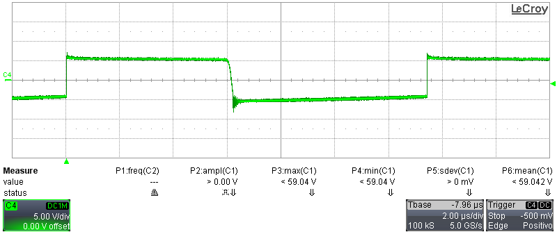
The switching waveforms in Figure 3-1 through Figure 3-3 were measured by supplying the converter at 5 V and 750-mA load, where the primary current reaches its highest peak, resulting into the highest spike on the SW-node.
 Figure 3-1 C2: Switch Node of U1 (TP2) (10 V/div, 2
μs/div, no BWL), VIN = 5 V
 Figure 3-2 C2: Switch Node of U1 (TP2) (10 V/div, 50
ns/div, no BWL), VIN = 5 V
 Figure 3-3 C4: Anode of D1 vs Secondary Ground (5 V/div, 2 μs/div, no BWL)