TIDT286 June   2022


  1.   Description
  2.   Features
  3.   Applications
  4. 1Test Prerequisites
    1. 1.1 Voltage and Current Requirements
    2. 1.2 Considerations
    3. 1.3 Dimensions
  5. 2Testing and Results
    1. 2.1 Efficiency Graph
    2. 2.2 Loss Graph
    3. 2.3 Load Regulation
    4. 2.4 Line Regulation
    5. 2.5 Thermal Images
      1. 2.5.1 0.5-A Output Current
      2. 2.5.2 1-A Output Current
      3. 2.5.3 1.5-A Output Current
      4. 2.5.4 2-A Output Current
      5. 2.5.5 Pulsed Ouput Current
    6. 2.6 Bode Plots
      1. 2.6.1 6-V Input Voltage
      2. 2.6.2 12-V Input Voltage
  6. 3Waveforms
    1. 3.1 Switching
      1. 3.1.1 Transistor Q1
        1. 3.1.1.1 Drain - Source
        2. 3.1.1.2 Gate - Source
      2. 3.1.2 Diode D3
    2. 3.2 Input Voltage Ripple
      1. 3.2.1 20-MHz Bandwidth
      2. 3.2.2 Full Bandwidth
    3. 3.3 Output Voltage Ripple
    4. 3.4 Load Transients
      1. 3.4.1 Switching Load From 1 A to 2 A
      2. 3.4.2 Switching Load From 0.2 A to 2 A
        1. 3.4.2.1 50% Duty Cycle
        2. 3.4.2.2 Low Duty Cycle (TON = 3 ms; TOFF = 30 ms)
    5. 3.5 Start-Up Sequence
    6. 3.6 Shutdown Sequence

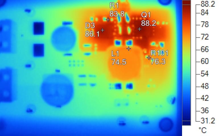
2-A Output Current

GUID-20220524-SS0I-DJKH-R7PL-MH3HJLBSGWTX-low.jpg Figure 2-9 IR Photo With 2-A Maximum Output Current
Note:

The thermal measurements show that the power stage itself is able to withstand a continuous load higher than 1 A.

At custom pulsed load, the temperature rise of the power stage is around dT = +20K.