TIDT293 October   2022


  1.   Description
  2.   Features
  3.   Applications
  4. 1Design Variants
  5. 2Design Overview
    1. 2.1 Board Contents
    2. 2.2 Connector Description
    3. 2.3 User Interface
      1. 2.3.1 Switches and Push-buttons
      2. 2.3.2 Jumpers
      3. 2.3.3 Potentiometers
    4. 2.4 Functional Block Diagram
    5. 2.5 Functional Block Descriptions
  6. 3Features and Performance Curves
    1. 3.1  Test Setup
    2. 3.2  Pulse
    3. 3.3  Levels and Free Run
    4. 3.4  INP
    5. 3.5  Dual-Output Power Supply
    6. 3.6  Overtemperature Protection
    7. 3.7  Slew Rate Adjust
    8. 3.8  Settling Time Adjust
    9. 3.9  Low- and High-Level Adjust
    10. 3.10 Pulse-Width Adjust
    11. 3.11 Period and Delay Adjust
    12. 3.12 Frequency Response
  7. 4Operation
    1. 4.1 Initial Setup – Jumper Selection and Potentiometer Settings
    2. 4.2 Procedure
      1. 4.2.1 Initial Power Up
      2. 4.2.2 Connecting the Circuit Under Test
  8. 5Limitations and Capabilities
    1. 5.1 Wiring Inductance
    2. 5.2 Minimum Voltage
    3. 5.3 Battery Life
  9. 6Typical Failure Mechanism
    1. 6.1 Fast Thermal Failure
    2. 6.2 Slow Thermal Failure

Minimum Voltage

In higher voltage versions, the minimum voltage is limited for the circuit under test due to a higher reference voltage. Testing at a lower output voltage does not allow enough voltage on the FET during the droop. This is also a limitation of the wiring inductance in the setup. Use short wires soldered directly to the load-step board to reduce wiring inductance. The results shown in the following waveform use a PSMN008-75B MOSFET in the 125-A, 50-V variant. The following scope plot is a 1-A to 25-A load transient for a 5-V output exhibiting an abnormal result.

GUID-20220531-SS0I-LXVD-H94H-68RXPFCWQLXN-low.pngFigure 5-3 1 A to 25 A, 5-V Output Load Transient

Applying a higher voltage does not collapse the FET voltage and creates a normal load transient. The following scope plot is a 1-A to 25-A load transient with a 10-V output.
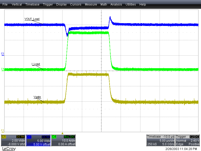
GUID-20220531-SS0I-VLRZ-Q90G-Z3GSRQ4XHCGJ-low.pngFigure 5-4 1-A to 25-A, 10-V Output Load Transient