TIDT293 October 2022
3.3 Levels and Free Run
The load step board has three step levels: a low level, a high level, and a zero level. In one cycle, the board starts at the zero level, steps up to the low level, and then to the high level. Afterwards, the load steps down to the low level and then to the zero level, until the next cycle.
The following scope plot shows a load transient of 10 A to 25 A at a 10 VOUT load. The low-level period is set for 14 ms, while the high-level pulse width is set for 4 ms. The results in the following waveform use a PSMN008-75B MOSFET in the 125-A, 50-V variant.
 Figure 3-6 High-, Low-, Zero-Level Step, 10 A to 25 A, 10-V Output Load Transient
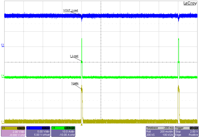
When the jumper, Free Run (J6), is installed, a free running pulse signal of 1 Hz triggers the sub-circuits necessary for a load transient. The following scope plot shows two cycles generated by the free run. The transient is a 10-A to 25-A load step for a 10-V output load. The results in the following waveform use a PSMN008-75B MOSFET in the 125-A, 50-V variant.
 Figure 3-7 Free Run, 10 A to 25 A, 10-VOUT Load Transient
When the jumper, Disable Zero (J7), is installed, the zero-level step is disabled during the load transient. The load stays at the adjusted low level until the next cycle. The following scope plot shows the load step board with the zero-level step disabled. The results in the following waveform use a PSMN008-75B MOSFET in the 125-A, 50-V variant. The zero-level is intended to keep the average power dissipation in Q2 within the safe operating area (SOA). Be sure to check the intended power through Q2 before installing J7.
 Figure 3-8 Disable Zero, 1 A to 5 A, 11 µs, 5-V Output Load Transient