TIDT295 August 2022
2.3 Thermal Images
All images were captured with the unit under test (UUT) enclosed in a 30 cm × 45 cm × 20 cm plexiglass box, 25ºC ambient, after a 30-minute warm up.
Figure 2-4 through Figure 2-7 illustrate the charge mode thermal images.
 Figure 2-4 20 VBUS and 20
VBAT Full Charging Mode
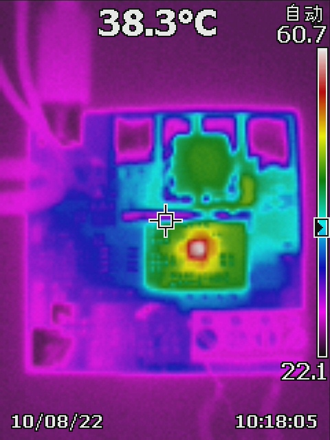 Figure 2-6 9 VBUS and 20
VBAT Full Charging Mode
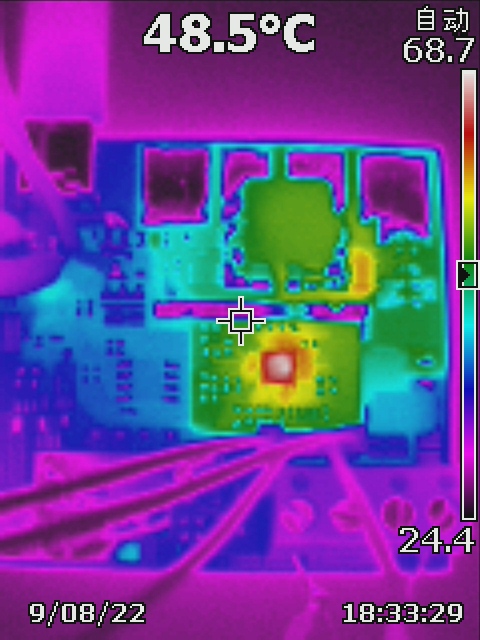 Figure 2-5 15 VBUS and 20
VBAT Full Charging Mode
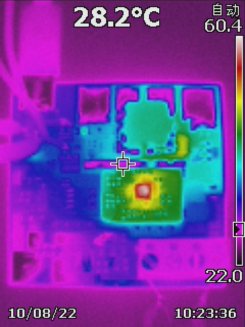 Figure 2-7 5 VBUS and 20
VBAT Full Charging Mode
Figure 2-7 5 VBUS and 20
VBAT Full Charging ModeFigure 2-8 through Figure 2-10 illustrate the OTG mode thermal images.
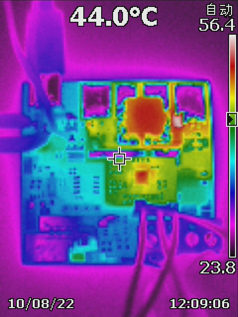 Figure 2-8 18 VBAT to 9 V,
3 A OTG Full Load
 Figure 2-10 18 VBAT to 20
V, 3 A OTG Full Load
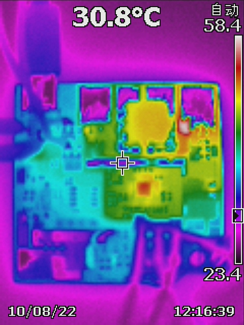 Figure 2-9 18 VBAT to 15
V, 3 A OTG Full Load