TIDT295 August 2022
3.2 Output Voltage Ripple and Noise
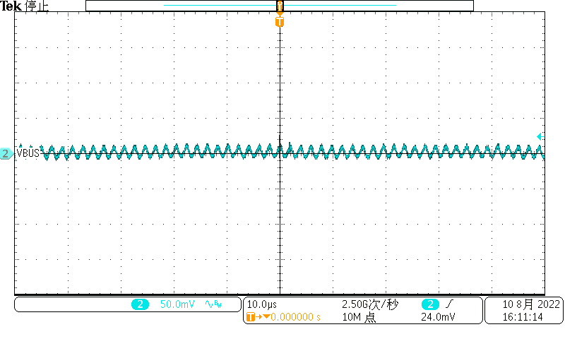
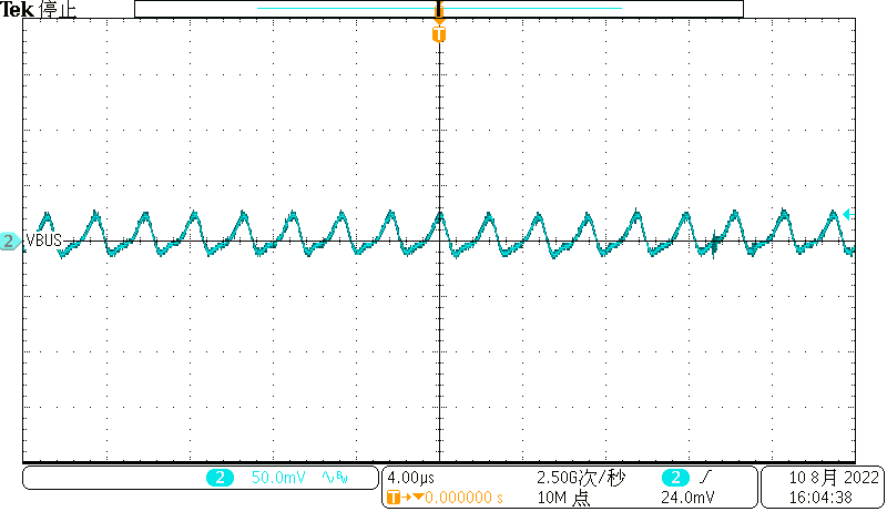
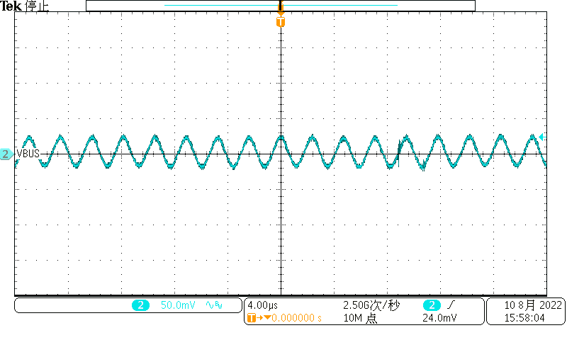
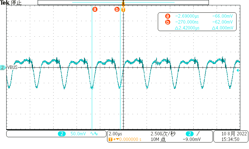
Output voltage ripple is shown in the following figures.
 Figure 3-9 VBAT 18 V to 5 V, 3 A Full-Load
Ripple at OTG Mode
 Figure 3-11 VBAT 18 V to 15 V, 3 A Full-Load
Ripple at OTG Mode
 Figure 3-10 VBAT 18 V to 9 V, 3 A Full-Load
Ripple at OTG Mode
 Figure 3-12 VBAT 18 V to 20 V, 3 A Full-Load
Ripple at OTG Mode