TIDT296 September 2022
3.3 Output Voltage Ripple
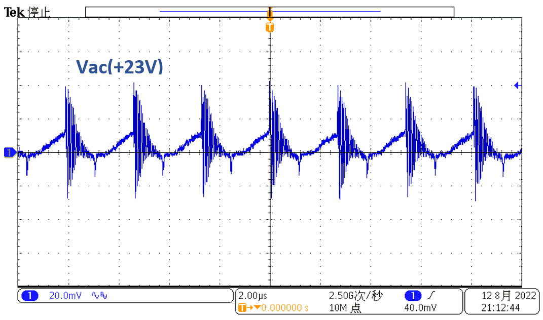
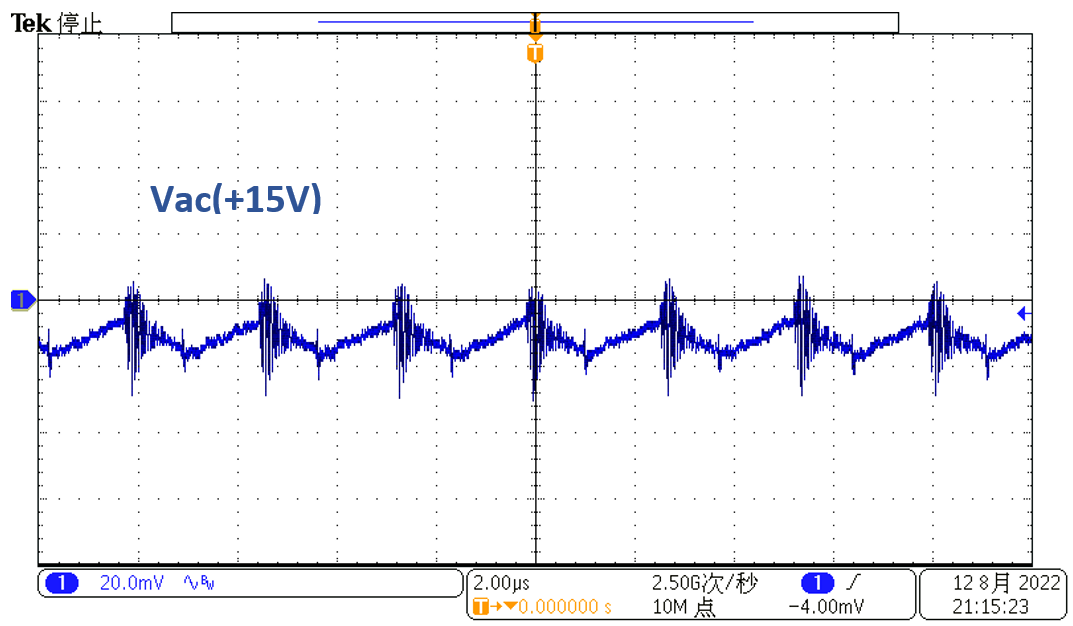
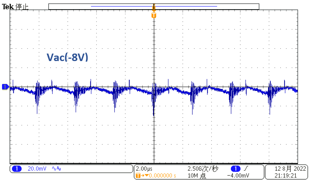
Figure 3-5 through Figure 3-7 show the output voltage ripple waveforms at the conditions indicated in the image title.
 Figure 3-5 VOUT1 +23-V Output Ripple,
VIN = 12 V, IOUT1 = 80 mA, IOUT2 = 80
mA
 Figure 3-6 VOUT1 +15-V Output Ripple,
VIN = 12 V, IOUT1 = 80 mA, IOUT2 = 80
mA
 Figure 3-7 VOUT1 –8-V Output Ripple,
VIN = 12 V, IOUT1 = 80 mA, IOUT2 = 80
mA