TIDT308 October   2022


  1.   Description
  2.   Features
  3.   Applications
  4. 1Test Prerequisites
    1. 1.1 Voltage and Current Requirements
    2. 1.2 Required Equipment
    3. 1.3 Considerations
    4. 1.4 Dimensions
    5. 1.5 Test Setup
  5. 2Testing and Results
    1. 2.1 Efficiency Graphs
    2. 2.2 Efficiency Data
    3. 2.3 Thermal Images
      1. 2.3.1 Top Side
      2. 2.3.2 Bottom Side
    4. 2.4 Bode Plots
  6. 3Waveforms
    1. 3.1 Switching
      1. 3.1.1 Secondary Side
      2. 3.1.2 Primary Side
        1. 3.1.2.1 Transistor Q8 Drain-Source
        2. 3.1.2.2 HS2-Pin of U1
          1. 3.1.2.2.1 Undershoot
          2. 3.1.2.2.2 Overshoot
    2. 3.2 Output Voltage Ripple
    3. 3.3 Load Transients
    4. 3.4 Start-Up Sequence
      1. 3.4.1 Full Load
      2. 3.4.2 Zero Load
      3. 3.4.3 Overload
    5. 3.5 Shutdown Sequence

Efficiency Graphs

Figure 2-1 shows the efficiency graph of the power supply versus output current. The input voltage has been set to 18 VDC, 24 VDC, and 30 VDC.
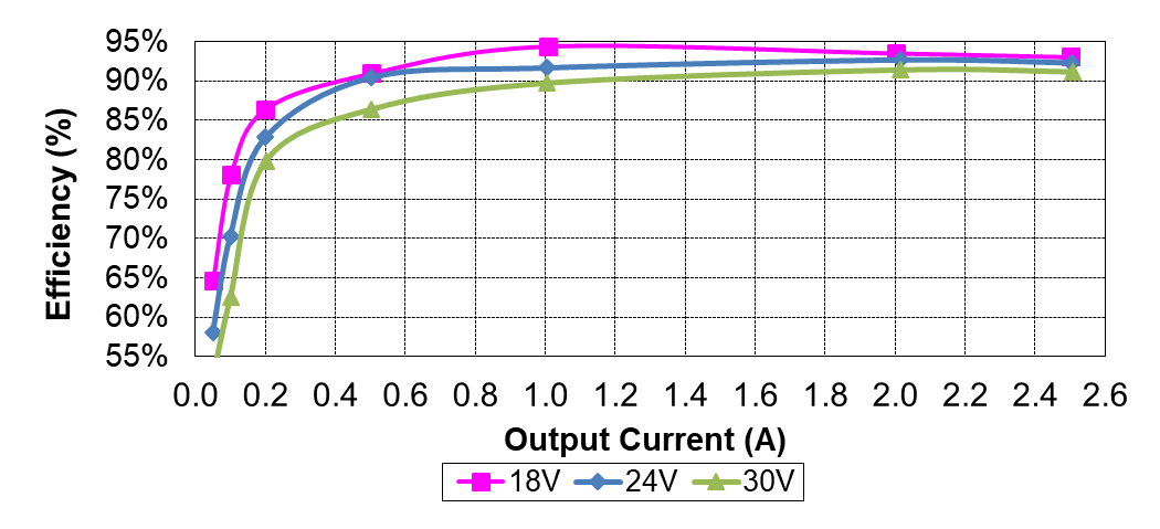
GUID-20220926-SS0I-M5PL-GNBV-KV5TP6VVDMD3-low.png Figure 2-1 Efficiency Graph