TIDT308 October   2022


  1.   Description
  2.   Features
  3.   Applications
  4. 1Test Prerequisites
    1. 1.1 Voltage and Current Requirements
    2. 1.2 Required Equipment
    3. 1.3 Considerations
    4. 1.4 Dimensions
    5. 1.5 Test Setup
  5. 2Testing and Results
    1. 2.1 Efficiency Graphs
    2. 2.2 Efficiency Data
    3. 2.3 Thermal Images
      1. 2.3.1 Top Side
      2. 2.3.2 Bottom Side
    4. 2.4 Bode Plots
  6. 3Waveforms
    1. 3.1 Switching
      1. 3.1.1 Secondary Side
      2. 3.1.2 Primary Side
        1. 3.1.2.1 Transistor Q8 Drain-Source
        2. 3.1.2.2 HS2-Pin of U1
          1. 3.1.2.2.1 Undershoot
          2. 3.1.2.2.2 Overshoot
    2. 3.2 Output Voltage Ripple
    3. 3.3 Load Transients
    4. 3.4 Start-Up Sequence
      1. 3.4.1 Full Load
      2. 3.4.2 Zero Load
      3. 3.4.3 Overload
    5. 3.5 Shutdown Sequence

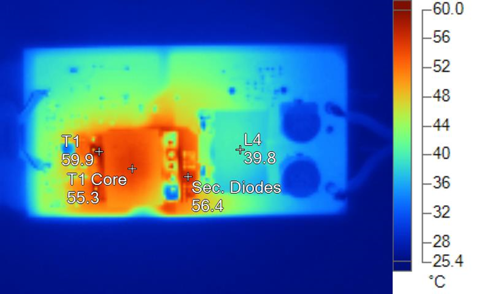
Top Side

GUID-20220926-SS0I-TQXT-MQR4-Z33KH1JLQXL2-low.png Figure 2-2 Thermal Image: Top View
Table 2-4 Main Image Markers
Name Temperature Emissivity Background
T1 59.9°C 0.96 25.5°C
T1 Core 55.3°C 0.96 25.5°C
Diodes (secondary side) 56.4°C 0.96 25.5°C
L4 39.8°C 0.96 25.5°C