TIDT315 December   2022


  1.   Description
  2.   Features
  3.   Applications
  4. 1Test Prerequisites
    1. 1.1 Voltage and Current Requirements
    2. 1.2 Considerations
    3. 1.3 Dimensions
  5. 2Testing and Results
    1. 2.1 Efficiency Graphs
    2. 2.2 Load Regulation
    3. 2.3 Thermal Images
      1. 2.3.1 Summary
      2. 2.3.2 Images With Thermal Interface Aluminum Adapter, Then Added Heat Sink to Adapter
      3. 2.3.3 Images Without Thermal Mechanics
      4. 2.3.4 Thermal Mechanics
        1. 2.3.4.1 Summary
        2. 2.3.4.2 Description – Mechanical Setup Needs a Workshop
    4. 2.4 Bode Plot
      1. 2.4.1 Bode Plot Using Quick Start Design Tool
      2. 2.4.2 Bode Plot Using Network Analyzer
  6. 3Waveforms
    1. 3.1 Switching
      1. 3.1.1 Overview of the Four Switching Phases
      2. 3.1.2 Low-Side FET
        1. 3.1.2.1 Switch Node to GND
        2. 3.1.2.2 Low-Side FET Gate to GND
      3. 3.1.3 High-Side FET
        1. 3.1.3.1 Switch Node to VIN
        2. 3.1.3.2 High-Side FET Gate to Switch Node
    2. 3.2 Output Voltage Ripple
    3. 3.3 Input Voltage Ripple
      1. 3.3.1 Power Stage Input
      2. 3.3.2 Board Input
    4. 3.4 Load Transients
      1. 3.4.1 Load Transient 10 A to 50 A
      2. 3.4.2 Load Transient 5 A to 50 A (90 %)
    5. 3.5 Start-Up Sequence
    6. 3.6 Shutdown Sequence
  7.   A Individual Adjusting of the Rising Edge and Falling Edge With LM5143A
    1.     A.1 Both Gate Resistors Before Gate Shorted
    2.     A.2 2 × 3.32-Ω Resistors in Before Gate of the High-Side FET
    3.     A.3 2.21-Ω High and 4.75-Ω Low Resistor in Before Gate of the High-Side FET
  8.   B Thermal Behavior, Prototype in Vertical Position
    1.     B.1 Thermal Summary
    2.     B.2 Thermal Images PCB with Heat Sink and Prototype in the Vertical Position
  9.   C ON Demand – Assembly of Thermal Interface
    1.     C.1 Thermal Interface Example

Description – Mechanical Setup Needs a Workshop

The following list applies to a four layer board, single-side assembly to enable a heat sink;

  • The thermal foil was mounted to the bare PCB, using a cost-effective RSpro #707-5657 (H48-6 material), 3.2 W/mK, Iso 700 V/mm
  • 150 mm × 150 mm × 1 mm = fits for two prototypes, adhesive on both sides
  • Drill the aluminum adapter 150 mm × 75 mm × 5 mm accordingly to the PCB, 3.5-mm diameter holes
  • Drill heat sink, SK 58 75 SA 150 mm × 75 mm accordingly to the PCB, with 2.5-mm diameter holes and cut thread to M3
  • For EMI measurements, connect the screw in between ph1 or ph4 via ring eyelet to output ground J5
GUID-20221026-SS0I-QXPQ-JGZN-4LZCVSZRK8CQ-low.png
GUID-20221026-SS0I-QXPK-D8QV-DQ7WRXGPJPJP-low.png

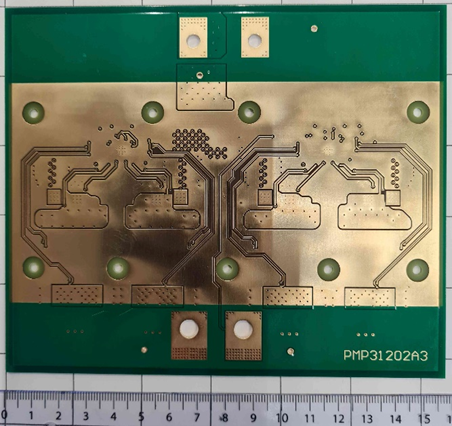
Bare PCB 150 mm × 125 mm - bottom side

No solder resist at heat sink area

Place thermal foil here

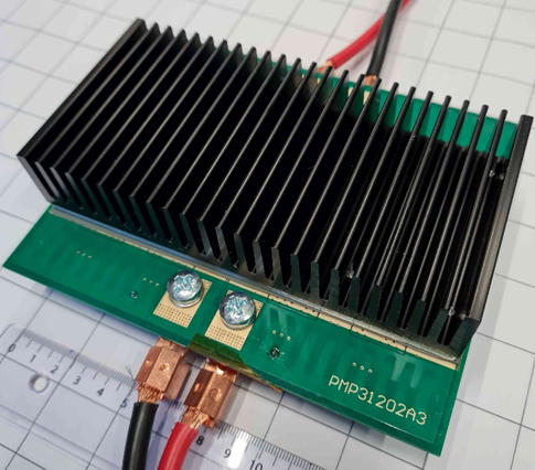
Standard heat sink 150 mm × 75 mm added to PCB

On top of aluminum adapter 150 mm × 75 mm × 5 mm

(The heat sink acts thermally like a metal case.)

For a more detailed description, see Appendix C.