TIDT315 December   2022


  1.   Description
  2.   Features
  3.   Applications
  4. 1Test Prerequisites
    1. 1.1 Voltage and Current Requirements
    2. 1.2 Considerations
    3. 1.3 Dimensions
  5. 2Testing and Results
    1. 2.1 Efficiency Graphs
    2. 2.2 Load Regulation
    3. 2.3 Thermal Images
      1. 2.3.1 Summary
      2. 2.3.2 Images With Thermal Interface Aluminum Adapter, Then Added Heat Sink to Adapter
      3. 2.3.3 Images Without Thermal Mechanics
      4. 2.3.4 Thermal Mechanics
        1. 2.3.4.1 Summary
        2. 2.3.4.2 Description – Mechanical Setup Needs a Workshop
    4. 2.4 Bode Plot
      1. 2.4.1 Bode Plot Using Quick Start Design Tool
      2. 2.4.2 Bode Plot Using Network Analyzer
  6. 3Waveforms
    1. 3.1 Switching
      1. 3.1.1 Overview of the Four Switching Phases
      2. 3.1.2 Low-Side FET
        1. 3.1.2.1 Switch Node to GND
        2. 3.1.2.2 Low-Side FET Gate to GND
      3. 3.1.3 High-Side FET
        1. 3.1.3.1 Switch Node to VIN
        2. 3.1.3.2 High-Side FET Gate to Switch Node
    2. 3.2 Output Voltage Ripple
    3. 3.3 Input Voltage Ripple
      1. 3.3.1 Power Stage Input
      2. 3.3.2 Board Input
    4. 3.4 Load Transients
      1. 3.4.1 Load Transient 10 A to 50 A
      2. 3.4.2 Load Transient 5 A to 50 A (90 %)
    5. 3.5 Start-Up Sequence
    6. 3.6 Shutdown Sequence
  7.   A Individual Adjusting of the Rising Edge and Falling Edge With LM5143A
    1.     A.1 Both Gate Resistors Before Gate Shorted
    2.     A.2 2 × 3.32-Ω Resistors in Before Gate of the High-Side FET
    3.     A.3 2.21-Ω High and 4.75-Ω Low Resistor in Before Gate of the High-Side FET
  8.   B Thermal Behavior, Prototype in Vertical Position
    1.     B.1 Thermal Summary
    2.     B.2 Thermal Images PCB with Heat Sink and Prototype in the Vertical Position
  9.   C ON Demand – Assembly of Thermal Interface
    1.     C.1 Thermal Interface Example

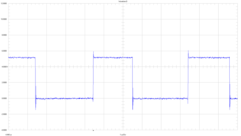
Low-Side FET Gate to GND

GUID-20221026-SS0I-VRFC-NMBF-KPP9HW8X7FZ9-low.png

2 V / div

1 µs / div

Full bandwidth

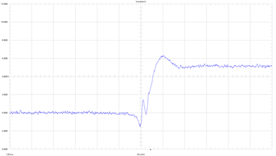
GUID-20221026-SS0I-9FNQ-DRWP-VMCJNVZC748B-low.png
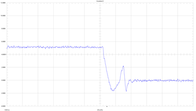
GUID-20221026-SS0I-1HR1-TBLL-WRXWHWX9R3KT-low.png

2 V / div

20 ns / div

Full bandwidth

Figure 3-3 Waveform Low-Side FET to GND