TIDT315 December   2022


  1.   Description
  2.   Features
  3.   Applications
  4. 1Test Prerequisites
    1. 1.1 Voltage and Current Requirements
    2. 1.2 Considerations
    3. 1.3 Dimensions
  5. 2Testing and Results
    1. 2.1 Efficiency Graphs
    2. 2.2 Load Regulation
    3. 2.3 Thermal Images
      1. 2.3.1 Summary
      2. 2.3.2 Images With Thermal Interface Aluminum Adapter, Then Added Heat Sink to Adapter
      3. 2.3.3 Images Without Thermal Mechanics
      4. 2.3.4 Thermal Mechanics
        1. 2.3.4.1 Summary
        2. 2.3.4.2 Description – Mechanical Setup Needs a Workshop
    4. 2.4 Bode Plot
      1. 2.4.1 Bode Plot Using Quick Start Design Tool
      2. 2.4.2 Bode Plot Using Network Analyzer
  6. 3Waveforms
    1. 3.1 Switching
      1. 3.1.1 Overview of the Four Switching Phases
      2. 3.1.2 Low-Side FET
        1. 3.1.2.1 Switch Node to GND
        2. 3.1.2.2 Low-Side FET Gate to GND
      3. 3.1.3 High-Side FET
        1. 3.1.3.1 Switch Node to VIN
        2. 3.1.3.2 High-Side FET Gate to Switch Node
    2. 3.2 Output Voltage Ripple
    3. 3.3 Input Voltage Ripple
      1. 3.3.1 Power Stage Input
      2. 3.3.2 Board Input
    4. 3.4 Load Transients
      1. 3.4.1 Load Transient 10 A to 50 A
      2. 3.4.2 Load Transient 5 A to 50 A (90 %)
    5. 3.5 Start-Up Sequence
    6. 3.6 Shutdown Sequence
  7.   A Individual Adjusting of the Rising Edge and Falling Edge With LM5143A
    1.     A.1 Both Gate Resistors Before Gate Shorted
    2.     A.2 2 × 3.32-Ω Resistors in Before Gate of the High-Side FET
    3.     A.3 2.21-Ω High and 4.75-Ω Low Resistor in Before Gate of the High-Side FET
  8.   B Thermal Behavior, Prototype in Vertical Position
    1.     B.1 Thermal Summary
    2.     B.2 Thermal Images PCB with Heat Sink and Prototype in the Vertical Position
  9.   C ON Demand – Assembly of Thermal Interface
    1.     C.1 Thermal Interface Example

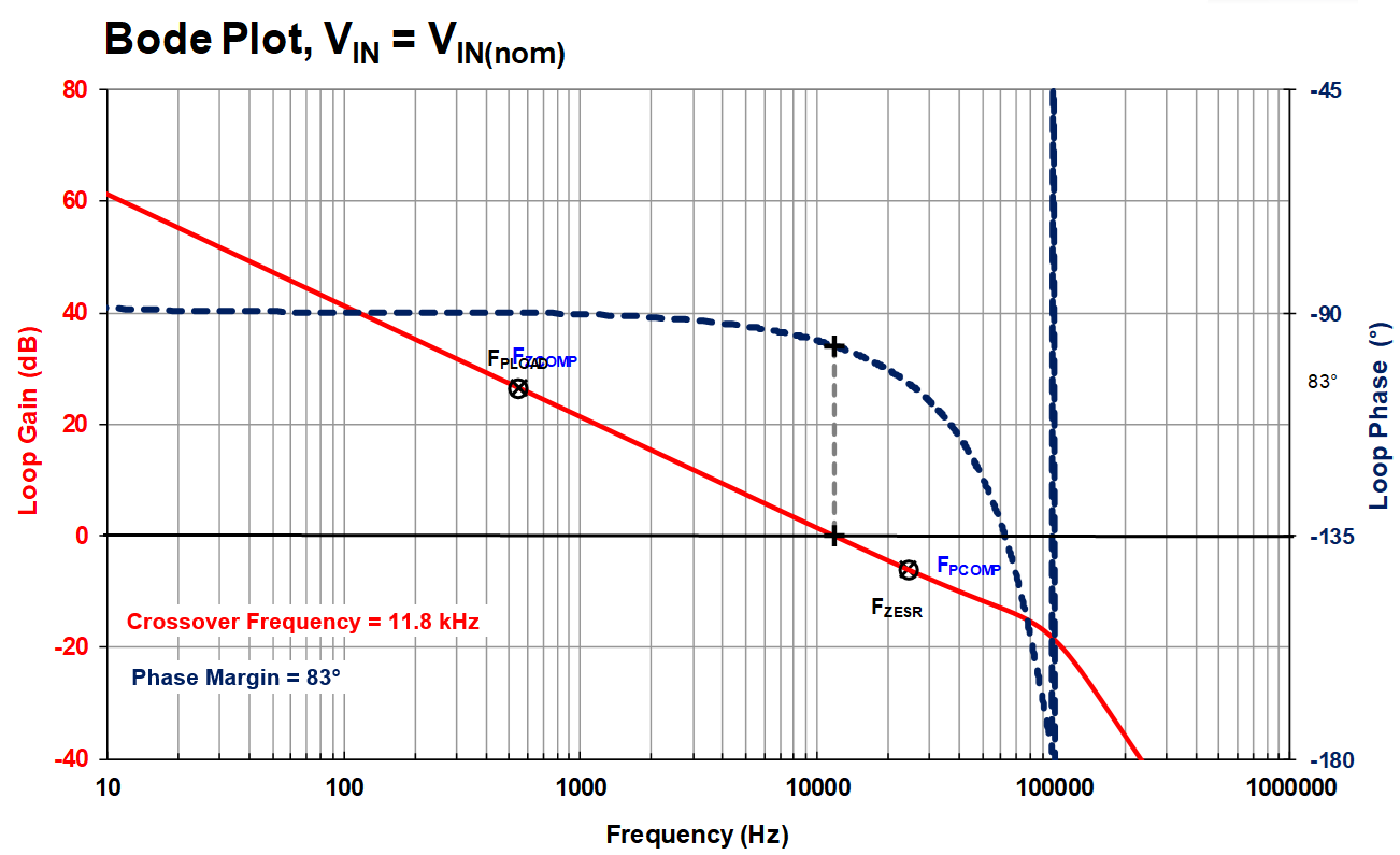
Bode Plot Using Quick Start Design Tool

GUID-20221028-SS0I-JP7S-R9NJ-N8W7ZKNGM0S3-low.png Figure 2-3 Bode Plot Derived From the Quick Start Design Tool

Download the quick start design tool from LM5143DESIGN-CALC.

Figure 2-3 is calculated for gain resistor 19.6 kΩ, zero capacitor 15 nF, and a pole capacitor of 330 pF at the error amplifier.

Figure 2-4 shows the matching measurement with VIN = 24 V and IOUT = 50 A.