TIDT316
December 2022
Description
Features
Applications
1
Test Prerequisites
1.1
Voltage and Current Requirements
1.2
Considerations
1.3
Dimensions
2
Testing and Results
2.1
Efficiency Graph
2.2
Loss Graph
2.3
Load Regulation
2.4
Line Regulation
2.5
Thermal Images
2.5.1
8-V Input Voltage
2.5.2
12-V Input Voltage
2.5.3
18-V Input Voltage
2.5.4
Conclusion
2.6
Bode Plots
2.6.1
5.2-V Input Voltage (Board Input, 5.0 V at Power Stage)
2.6.2
12-V Input Voltage
2.6.3
18-V Input Voltage
3
Waveforms
3.1
Switching
3.1.1
Switchnode (SW) to GND
3.1.1.1
8-V Input Voltage
3.1.1.2
12-V Input Voltage
3.1.1.3
18-V Input Voltage
3.1.2
Diode D1 (Referenced to VOUT)
3.1.2.1
8-V Input Voltage
3.1.2.2
12-V Input Voltage
3.1.2.3
18-V Input Voltage
3.2
Output Voltage Ripple
3.3
Input Voltage Ripple (AC-Coupled)
3.3.1
Board Input
3.3.2
Power Stage Input
3.4
Load Transients
3.4.1
8-V Input Voltage
3.4.2
12-V Input Voltage
3.4.3
18-V Input Voltage
3.5
Start-Up Sequence
3.5.1
8-V Input Voltage
3.5.2
12-V Input Voltage
3.5.3
18-V Input Voltage
3.6
Shutdown Sequence
3.6.1
8-V Input Voltage
3.6.2
12-V Input Voltage
3.6.3
18-V Input Voltage
A Output Ripple Reduction, Output Current Capability, and Dithering Option
A.1 Output Ripple Reduction by Adding Ceramic Output Capacitors (MLCCs)
A.1.1 Initial Design
A.1.2 Adding one 47-µF X7R Ceramic Capacitor, MLCC, 10 V, X7R, 1210
A.1.3 Adding a Second 47-µF Capacitor (Final Design)
A.2 Maximum Output Current Capability at Ultra-Low Cold Cranking Using LM5157
A.3 Dithering Option via Resistor R10
A.3.1 Enabled
A.3.2 Disabled
2.6.3
18-V Input Voltage
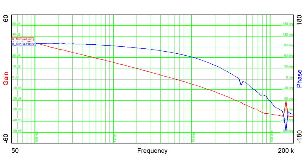
Figure 2-8
Bode Plot for 18-V Input Voltage and 2-A Output Current