TIDT318 January 2023
2.2 Thermal Images
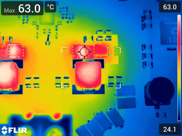
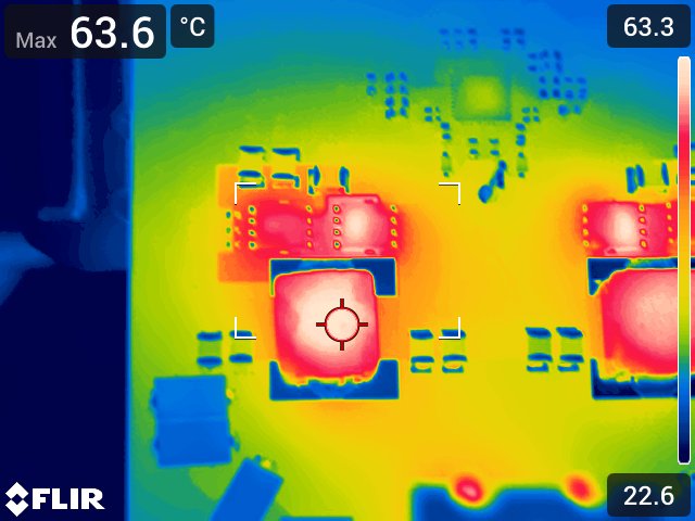
The first two thermal images in this section were taken with a load of 60 A, 14 VIN with a fan.
Figure 2-3 and Figure 2-4 show the thermal images of the board in phase 1 (Figure 2-3), followed by phase 2 (Figure 2-4). In these images, both low-side FETs and main inductors each had about a 40°C rise from the ambient room temperature of 21°C to 23°C.
 Figure 2-3 Phase 1 With Fan
 Figure 2-4 Phase 2 With Fan
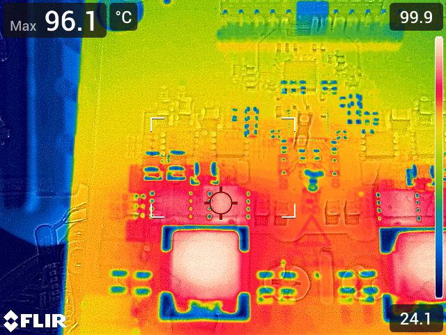
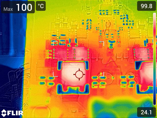
The thermal images in Figure 2-5 and Figure 2-6 are for the same 14 VIN, but no fan was used and the load was 45 A. Here, phase 2 (Figure 2-6) was slightly hotter than phase 1 (Figure 2-5) with the inductor reaching 100°C, and the low-side FET reaching 96°C from the same ambient room temperature of 21°C to 23°C.
 Figure 2-5 Phase 1 With No Fan
 Figure 2-6 Phase 2 With No Fan