TIDT320A january 2023 – july 2023
3.4 Thermal Images
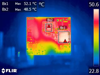
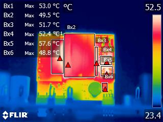
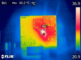
Thermal images are shown in the following figures. All images were captured with the unit under test (UUT) enclosed in a 30-cm × 45-cm × 20-cm Plexiglas box at 25ºC ambient, after a 30-minute warm up. For the full load images, the unit was tested with 390-VDC input, 3.7-A load on 12VSB and no load on P18V and S12V. Forced air was used, with the fan current limited to 200 mA. Table 3-8 summarizes the results of the full load images. In the OFF state image, the unit was tested with a 310-VDC input and DIS shorted to PGND. No forced air flow was used. The maximum temperature was 65.3°C, measured on the depletion mode start-up or sensing FET Q2.
| Reference Designator | Description | Maximum Temperature (°C) |
|---|---|---|
| U1 | LMG2610 GaN half-bridge | 52.1 |
| U3 | UCC28782 ACF controller | 48.5 |
| N/A | Planar transformer PCB near core on primary side | 53.0 |
| CORE50 | Planar transformer core | 49.5 |
| N/A | Planar transformer PCB near core on secondary side | 51.7 |
| Q50 | Synchronous rectifier FET | 52.4 |
| U50 | UCC24612 SR driver | 57.6 |
| R3 | Secondary current sense resistor | 48.8 |
 Figure 3-4 Thermal Image Full Load
(GaN-Side of Assembly)
 Figure 3-5 Thermal Image Full Load
(Transformer-Side of Assembly)
 Figure 3-6 Thermal Image OFF
State(GaN-Side of Assembly)