TIDT335 july 2023
2.1 Efficiency and Thermals
Table 2-1 shows the results of the boost converter efficiency testing. The output voltage was set to 8.5 V for all tests. 4.7 R was used as gate resistor for the switching MOSFET.
Table 2-1 Testing Results
| Input Voltage (V) | Output Current (A) | Efficiency (%) |
|---|---|---|
| 3.2 | 0.3 | 88.5 |
| 3.2 | 0.6 | 88.5 |
| 3.2 | 1 | 85.9 |
| 3.2 | 1.25 | 83.6 |
| 5 | 0.3 | 90.0 |
| 5 | 0.6 | 90.9 |
| 5 | 1 | 90.5 |
| 5 | 1.25 | 89.9 |
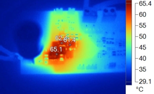
Thermal testing was performed with 3.2-V input voltage, 1.25-A output current at 25°C ambient temperature, board placed flat on the table, no artificial air flow. Figure 3-7 was taken after thermal equilibrium was reached.
 Figure 2-1 Thermal Image