TIDT336 may   2023


  1.   1
  2.   Description
  3.   Features
  4.   Applications
  5. 1Test Prerequisites
    1. 1.1 Voltage and Current Requirements
    2. 1.2 Required Equipment
    3. 1.3 Considerations
    4. 1.4 Dimensions
    5. 1.5 Test Setup
  6. 2Testing and Results
    1. 2.1 Efficiency Graph
    2. 2.2 Efficiency Data
    3. 2.3 Static Output Voltage Variation vs Load Current and VIN
      1. 2.3.1 24-V Output Voltage
      2. 2.3.2 3.3-V Output Voltage
      3. 2.3.3 U2 Input Voltage
  7. 3Waveforms
    1. 3.1 Switching Waveforms on Pin 1 of U1 (SW), Anodes of D1 and D4, at Full Load
      1. 3.1.1 18-V Input Voltage
      2. 3.1.2 24-V Input Voltage
      3. 3.1.3 32-V Input Voltage
    2. 3.2 Output Voltage Ripple
    3. 3.3 Load Transients
    4. 3.4 Start-Up Sequence
      1. 3.4.1 No Load
      2. 3.4.2 Full Load
    5. 3.5 Shutdown Sequence

Output Voltage Ripple

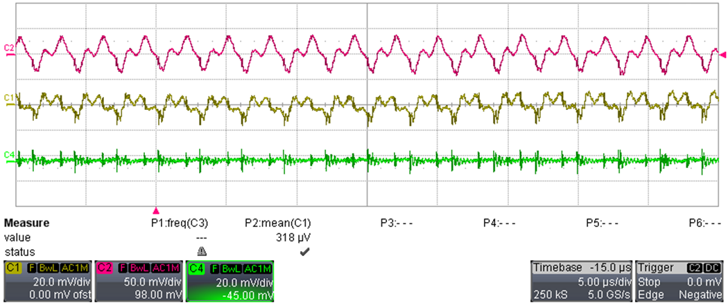
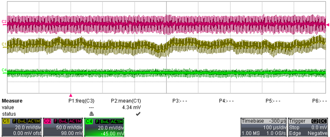
The 3.3-V and 24-V outputs, as well as input voltage and ripple were measured by supplying the converter at 24 VDC with both outputs loaded at nominal current. The bandwidth limit of the scope was set to 20 MHz, and the coupling to AC.
GUID-20230511-SS0I-LDPP-WVJD-86LXRC4SMLXX-low.png

C1: 24 VOUT

(20 mV / div)


C2: VIN

(50 mV / div)


C4: 3.3 VOUT

(20 mV / div)


(5 µs / div)

Figure 3-4 Output Voltage Ripple With 5 µs / div

Figure 3-5 is the same waveform as in Figure 3-10 but with longer time division for showing details about low-frequency ripple.
GUID-20230511-SS0I-RJBZ-FPZM-K3JCG0HDNLXF-low.png

C1: 24 VOUT

(20 mV / div)


C2: VIN

(50 mV / div)


C4: 3.3 VOUT

(20 mV / div)


(100 µs / div)

Figure 3-5 Output Voltage Ripple With 100 µs / div