TIDT343 October 2023
3.4 Load Transients
Load transient response waveforms are shown in the following figures.
Electronic load was used to create the load steps.
The output capacitors and compensation network need to be optimized according to the worst-case load step to meet the specific C2000 MCU supply requirements.
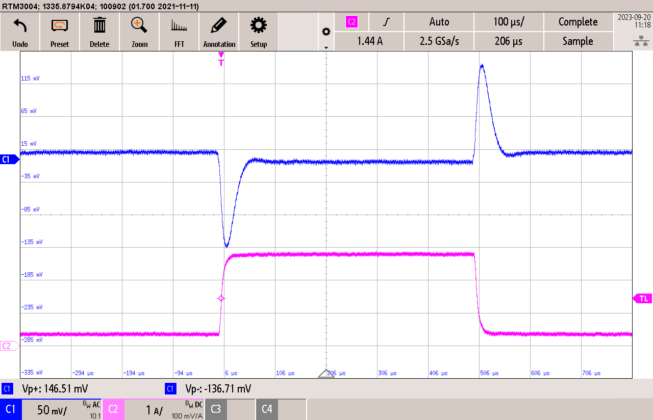
 Figure 3-7 Load Transient 1 (VIN = 12
V, CH1: VOUT1 = 3.3 V, CH2: IOUT1 = 0.3 → 2.7 A),
Figure 3-7 Load Transient 1 (VIN = 12
V, CH1: VOUT1 = 3.3 V, CH2: IOUT1 = 0.3 → 2.7 A),20-MHz Bandwidth Limited
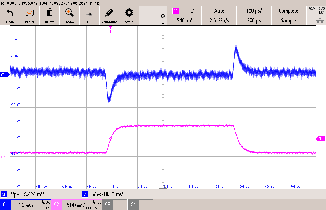
 Figure 3-8 Load Transient 2 (VIN = 3.3
V, CH1: VOUT2 = 1.2 V, CH2: IOUT2 = 0.1 → 0.9 A),
Figure 3-8 Load Transient 2 (VIN = 3.3
V, CH1: VOUT2 = 1.2 V, CH2: IOUT2 = 0.1 → 0.9 A),20-MHz Bandwidth Limited