TIDT343 October   2023


  1.   1
  2.   Description
  3.   Features
  4.   Applications
  5. 1Test Prerequisites
    1. 1.1 Voltage and Current Requirements
    2. 1.2 Dimensions
  6. 2Testing and Results
    1. 2.1 Efficiency Graphs
    2. 2.2 Efficiency Data
    3. 2.3 Thermal Images
    4. 2.4 Bode Plots
    5. 2.5 EMI
  7. 3Waveforms
    1. 3.1 Switching
    2. 3.2 Output Voltage Ripple
    3. 3.3 Input Voltage Ripple
    4. 3.4 Load Transients
    5. 3.5 Start-Up Sequence

Switching

Switching behavior is shown in the following figures.
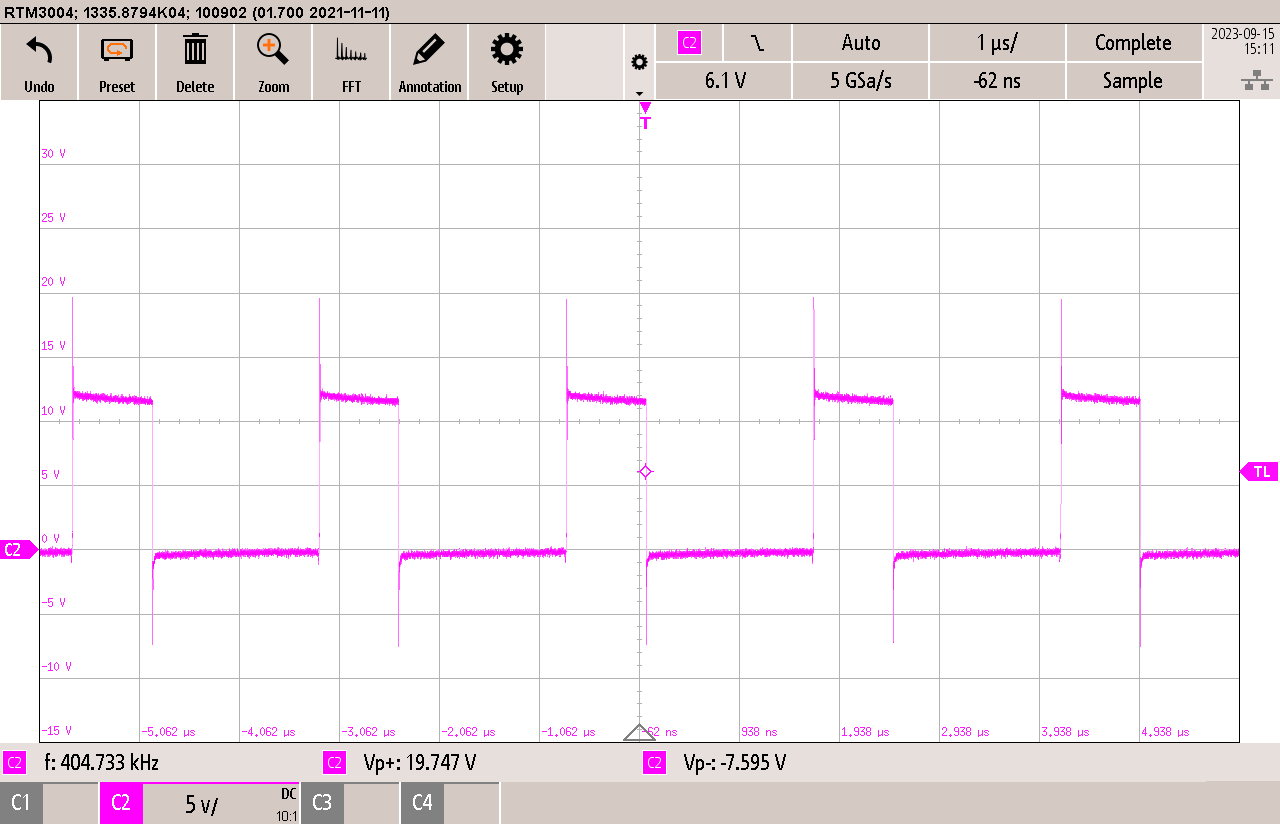
GUID-20230918-SS0I-JCL3-XDS3-8C6ZJJQGXV9Z-low.jpg Figure 3-1 Switching 1 (VIN = 12 V, VOUT1 = 3.3 V, IOUT1 = 3 A)
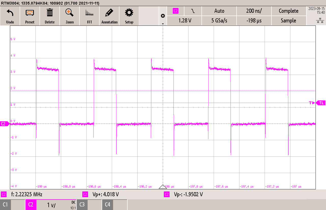
GUID-20230918-SS0I-RMMR-FHR5-XK1WSTXNTWG2-low.jpg Figure 3-2 Switching 2 (VIN = 3.3 V, VOUT2 = 1.2 V, IOUT2 = 1 A)