TIDT346 august   2023


  1.   1
  2.   Description
  3.   Features
  4.   Applications
  5. 1Test Prerequisites
    1. 1.1 Voltage and Current Requirements
    2. 1.2 Considerations
    3. 1.3 Dimensions
  6. 2Testing and Results
    1. 2.1 Efficiency Graphs
    2. 2.2 Efficiency Data
      1. 2.2.1 6-V Input Voltage
      2. 2.2.2 12-V Input Voltage
      3. 2.2.3 16-V Input Voltage
    3. 2.3 Thermal Images
    4. 2.4 Bode Plots
      1. 2.4.1 4.5-V Input Voltage
      2. 2.4.2 6-V Input Voltage
      3. 2.4.3 12-V Input Voltage
  7. 3Waveforms
    1. 3.1 Switching
      1. 3.1.1 6-V Input Voltage and 1-A Load
      2. 3.1.2 16-V Input Voltage and 1-A Load
      3. 3.1.3 Overshoot at VIN 12 V and 1-A Load Current
      4. 3.1.4 Undershoot at 12 VIN and 1-A Load Current
    2. 3.2 Output Voltage Ripple
    3. 3.3 Input Voltage Ripple
    4. 3.4 Load Transients
      1. 3.4.1 6-V Input Voltage
      2. 3.4.2 16-V Input Voltage
    5. 3.5 Start-Up Sequence (1-A Load)
    6. 3.6 Shutdown Sequence
      1. 3.6.1 No Load
      2. 3.6.2 1-A Load

Thermal Images

Thermal images were taken at an ambient temperature of 25°C without artificial airflow and the board was placed flat on the table.
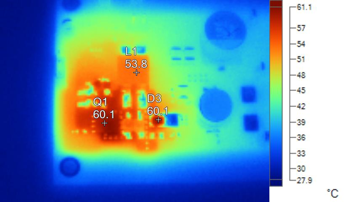
GUID-20230803-SS0I-LMXQ-HSMP-V38SMCJSR7KB-low.png Figure 2-2 4.5-V Input Voltage and 1-A Output Current
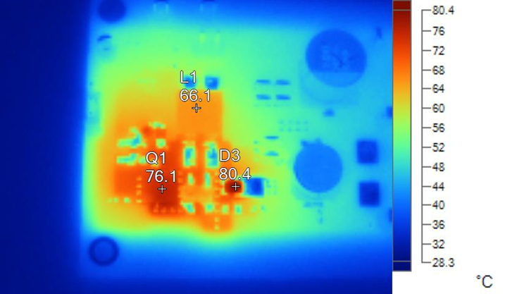
GUID-20230803-SS0I-TH1G-KKR7-NHGNVW26H5W0-low.png Figure 2-3 6-V Input Voltage and 1.5-A Output Current