TIDT348 august 2023
3.1 Switching Waveforms
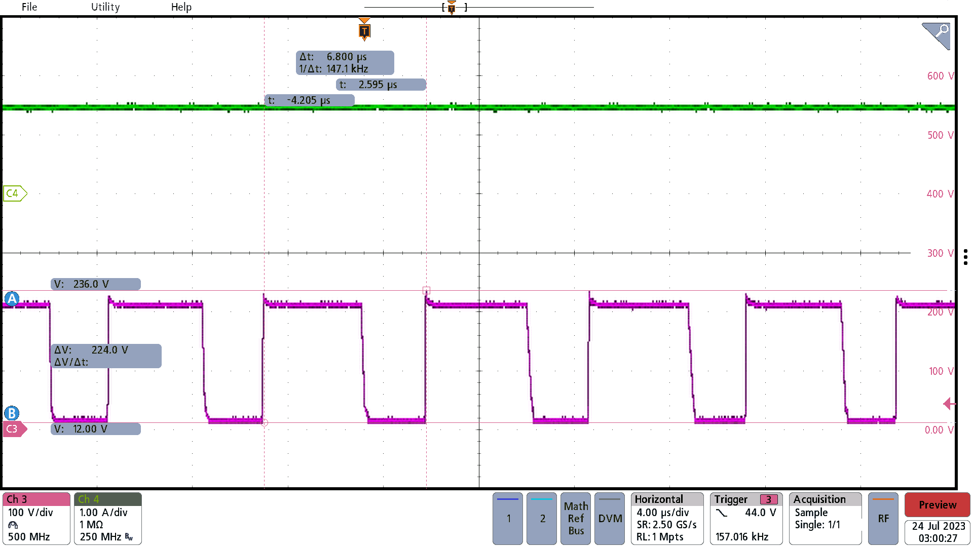
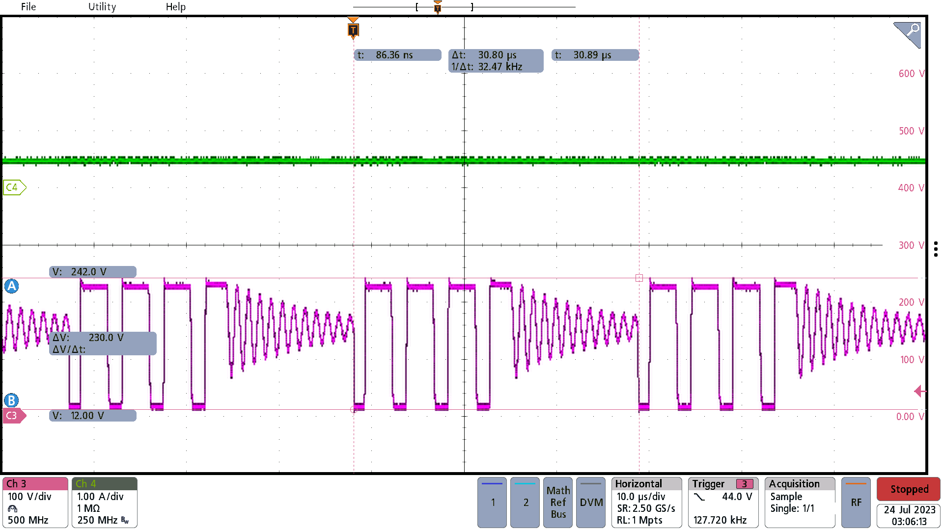
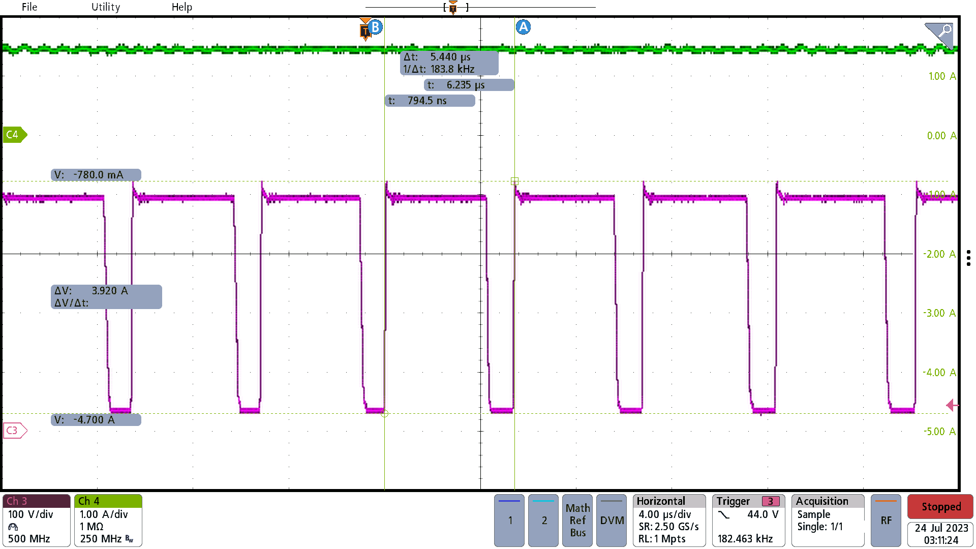
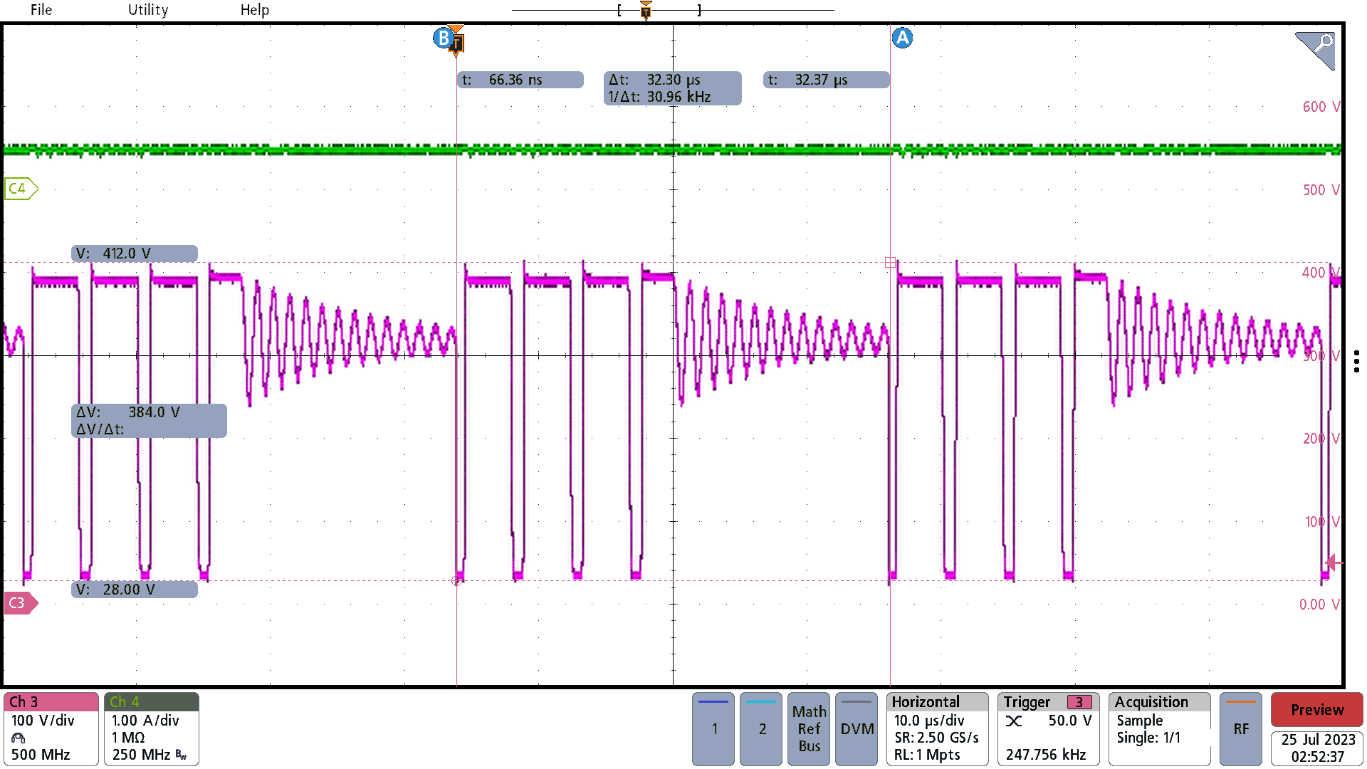
The following images illustrate the switching waveforms. The channels are identified with the following:
C3 = Q2 Vds, C2 = 12-V output current
 Figure 3-1 115-Vac Input, 12-V Loaded to
1.5 A
 Figure 3-2 115-Vac Input, 12-V Loaded to
0.5 A
 Figure 3-3 230-Vac Input, 12-V Loaded to
1.5 A
 Figure 3-4 230-Vac Input, 12-V Loaded to
0.5 A