TIDT350 October   2023


  1.   1
  2.   Description
  3.   Features
  4.   Applications
  5. 1Test Prerequisites
    1. 1.1 Voltage and Current Requirements
    2. 1.2 Considerations
    3. 1.3 Dimensions
  6. 2Testing and Results
    1. 2.1 Efficiency and Load Regulation Graphs
      1. 2.1.1 Symmetrical Load
        1. 2.1.1.1 Efficiency and Loss
        2. 2.1.1.2 Load Regulation
      2. 2.1.2 Nonsymmetrical Load
        1. 2.1.2.1 One Output 50 mA, Other Output Varying
          1. 2.1.2.1.1 Efficiency
          2. 2.1.2.1.2 Loss
          3. 2.1.2.1.3 Load Regulation
            1. 2.1.2.1.3.1 Positive Output Voltage
            2. 2.1.2.1.3.2 Negative Output Voltage
        2. 2.1.2.2 One Output Loaded With 1 kΩ, Other Output is Varying
          1. 2.1.2.2.1 Efficiency
          2. 2.1.2.2.2 Loss
          3. 2.1.2.2.3 Load Regulation
            1. 2.1.2.2.3.1 Positive Output Voltage
            2. 2.1.2.2.3.2 Negative Output Voltage
      3. 2.1.3 Scaling the Output Voltage
    2. 2.2 Thermal Images
    3. 2.3 Bode Plots With Dynamic Voltage Scaling
  7. 3Waveforms
    1. 3.1 Switching
      1. 3.1.1 Switchnode SW-GND
      2. 3.1.2 SW to P_OUT (D1)
      3. 3.1.3 Waveform on D3 Referenced to N_OUT
    2. 3.2 Output Voltage Ripple
      1. 3.2.1 Positive Output Voltage (P_OUT)
      2. 3.2.2 Negative Output Voltage (N_OUT)
    3. 3.3 Input Voltage Ripple
    4. 3.4 Load Transients
    5. 3.5 Start-Up Sequence
    6. 3.6 Shutdown Sequence

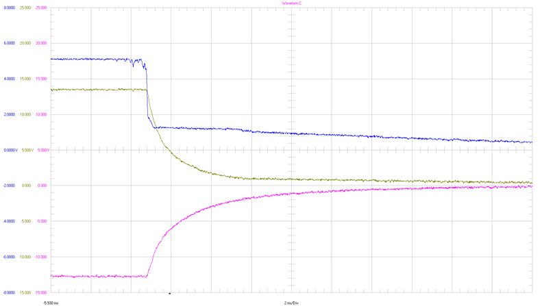
Shutdown Sequence

GUID-20230822-SS0I-TX4T-3NRS-XH867GMBHKRW-low.png

Input Voltage (blue)

2 V / div


Output P_OUT

5 V / div


Output N_OUT

5 V / div


2 ms / div

20-MHz bandwidth

Figure 3-9 Shutdown Sequence