TIDT351 September   2023


  1.   1
  2.   Description
  3.   Features
  4.   Applications
  5. 1Test Prerequisites
    1. 1.1 Voltage and Current Requirements
    2. 1.2 Considerations
    3. 1.3 Dimensions
  6. 2Testing and Results
    1. 2.1 Efficiency and Loss Graph
      1. 2.1.1 Efficiency
      2. 2.1.2 Loss
    2. 2.2 Load Regulation
      1. 2.2.1 18-V Output Voltage (VOUT-A)
      2. 2.2.2 12-V Output Voltage (VOUT-B)
    3. 2.3 Line Regulation
      1. 2.3.1 18-V Output Voltage (VOUT-A)
      2. 2.3.2 12-V Output Voltage (VOUT-B)
      3. 2.3.3 Efficiency and Loss vs Line Variation
    4. 2.4 Cross Regulation
      1. 2.4.1 12-V Output With No Load
        1. 2.4.1.1 Effects on the 18-V Output
        2. 2.4.1.2 Effects on the 12-V Output
      2. 2.4.2 18-V Output With no Load
        1. 2.4.2.1 Effects on the 12-V Output Voltage
        2. 2.4.2.2 Effects on the 18-V Output Voltage
    5. 2.5 Thermal Images
  7. 3Waveforms
    1. 3.1 Switching
      1. 3.1.1 Primary Switching Node
        1. 3.1.1.1 8-V Input Voltage
          1. 3.1.1.1.1 Full Load
          2. 3.1.1.1.2 No Load
        2. 3.1.1.2 36-V Input Voltage
          1. 3.1.1.2.1 Full Load
          2. 3.1.1.2.2 No Load
      2. 3.1.2 Diode D3 Referenced to VOUT-B (12 V)
        1. 3.1.2.1 8-V Input Voltage
          1. 3.1.2.1.1 Full Load
          2. 3.1.2.1.2 No Load
        2. 3.1.2.2 36-V Input Voltage
          1. 3.1.2.2.1 Full Load
          2. 3.1.2.2.2 No Load
      3. 3.1.3 Diode D4 Referenced to VOUT-A (18 V)
        1. 3.1.3.1 8-V Input Voltage
          1. 3.1.3.1.1 Full Load
          2. 3.1.3.1.2 No Load
        2. 3.1.3.2 36-V Input Voltage
          1. 3.1.3.2.1 Full Load
          2. 3.1.3.2.2 No Load
    2. 3.2 Input Voltage Ripple
    3. 3.3 Output Voltage Ripple
      1. 3.3.1 VOUT-A (18 V)
      2. 3.3.2 VOUT-B (12 V)
    4. 3.4 Load Transients
      1. 3.4.1 Switching on VOUT-A (18 V)
        1. 3.4.1.1 Effects on VOUT-A
        2. 3.4.1.2 Effects on VOUT-B
      2. 3.4.2 Switching on VOUT-B (12 V)
        1. 3.4.2.1 Effects on VOUT-B
        2. 3.4.2.2 Effects on VOUT-A
    5. 3.5 Start-Up Sequence
      1. 3.5.1 Full Load
      2. 3.5.2 No Load
    6. 3.6 Shutdown Sequence
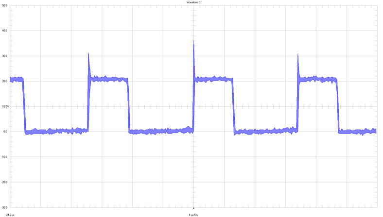
Full Load
GUID-20230823-SS0I-R4F3-P74P-DXVBZLJXJWM2-low.png

10 V / div

4 µs / div

full bandwidth

73 kHz

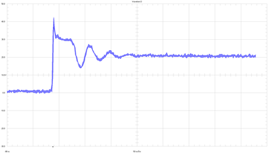
GUID-20230823-SS0I-WVMC-28GR-SXKKBJXXZKJR-low.png
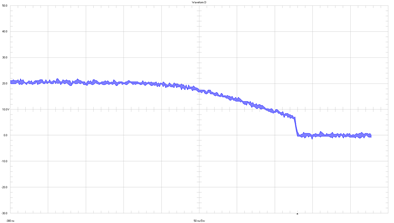
GUID-20230823-SS0I-RMRG-LSMP-9HTRT1XXQSSC-low.png

10 V / div

50 ns / div

full bandwidth

Figure 3-1 Primary Switch Node, 8 VIN, Full Load