TIDT355 October 2023
3.1 Switching
Switching behavior is shown in the following figures.
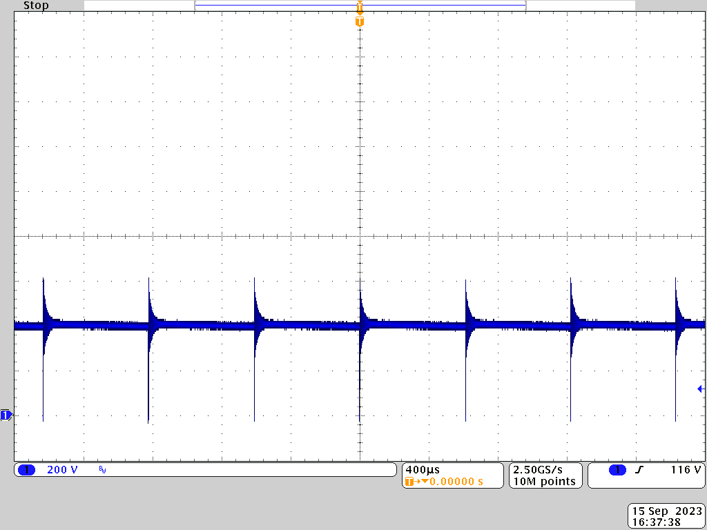 Figure 3-1 VDS of Low-Side
Switch at 600 VIN,
Figure 3-1 VDS of Low-Side
Switch at 600 VIN,0-A Load
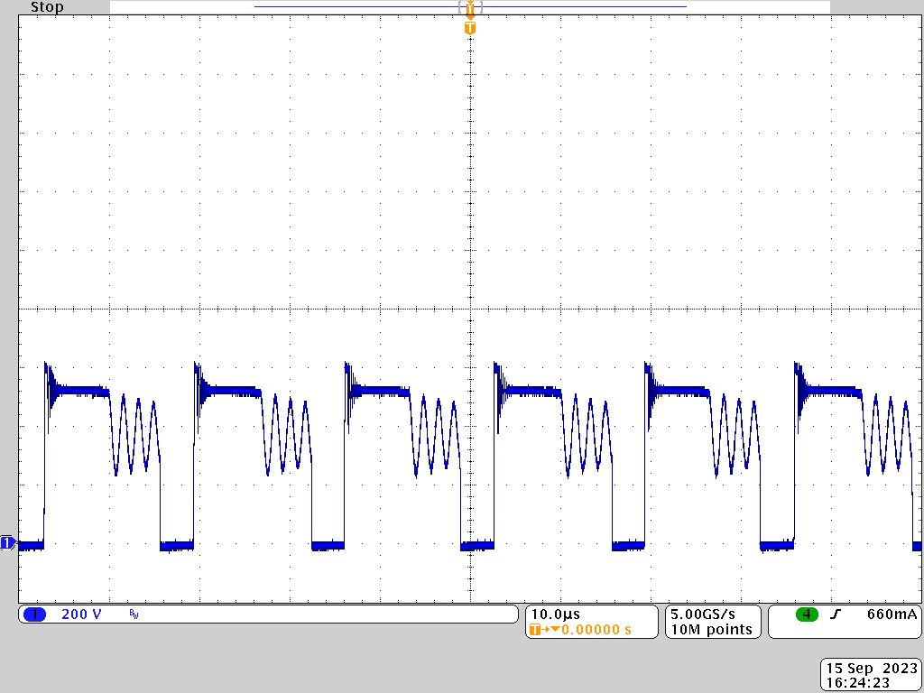 Figure 3-3 VDS of Low-Side
Switch Zoom at
Figure 3-3 VDS of Low-Side
Switch Zoom at600 VIN, Full Load
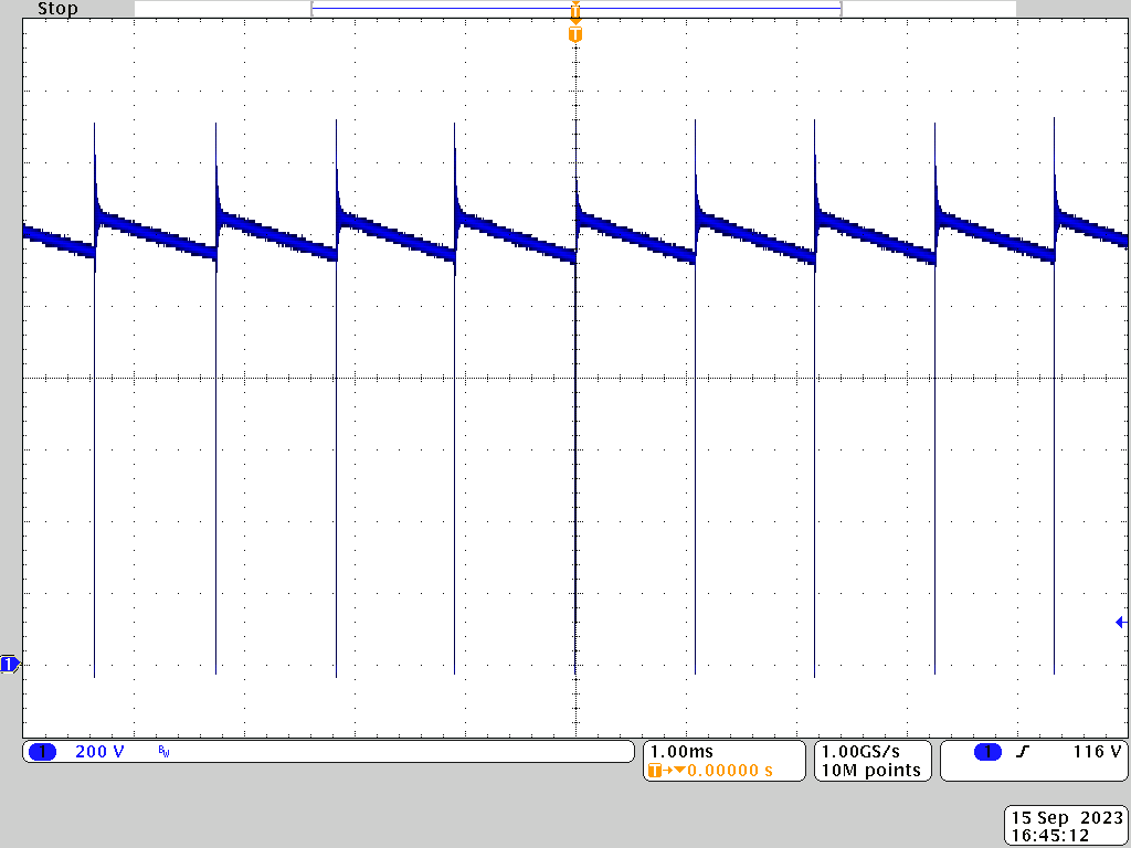 Figure 3-5 VDS of Low-Side
Switch at 1500 VIN,
Figure 3-5 VDS of Low-Side
Switch at 1500 VIN,0-A Load
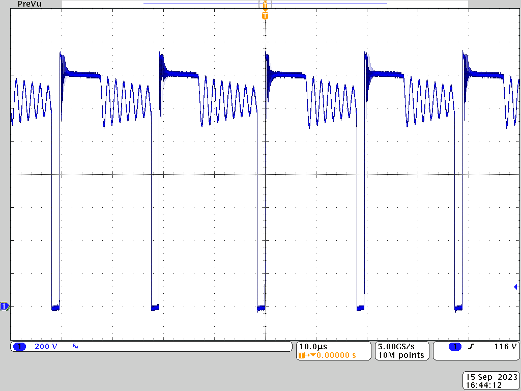
CH1: VDS of
Low-Side Switch at 1500 VIN Full Load
Figure 3-7 VDS of Low-Side
Switch at 1500 VIN,Full Load
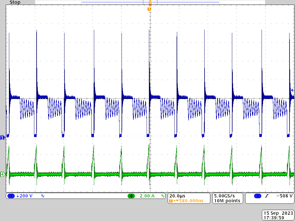
CH1: VDS of
High-Side Switch at 1500 VIN, Full Load
CH4: Primary current
Figure 3-9 VDS of
High-Side Switch atCH4: Primary current
1500 VIN, Full Load
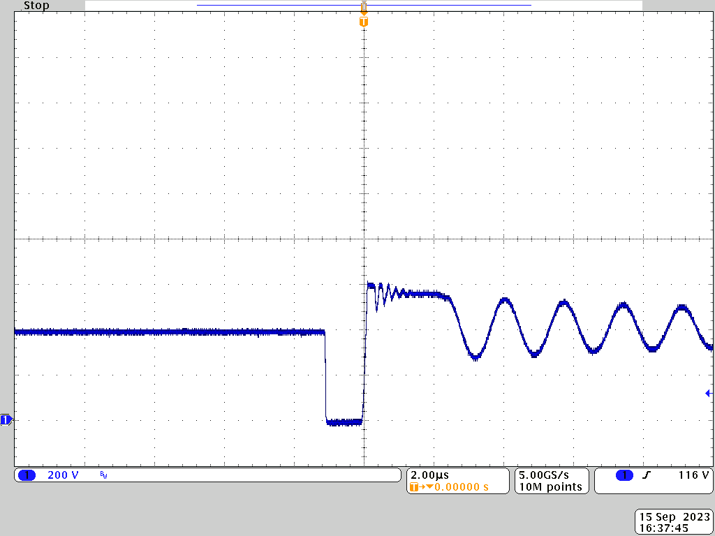 Figure 3-2 VDS of Low-Side
Switch Zoom at
Figure 3-2 VDS of Low-Side
Switch Zoom at600 VIN, 0-A Load
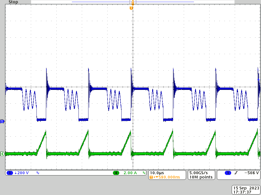
CH1: VDS of
High-Side Switch at 600 VIN, Full Load
CH4: Primary Current
Figure 3-4 High-Side Switch at 600
VIN, Full LoadCH4: Primary Current
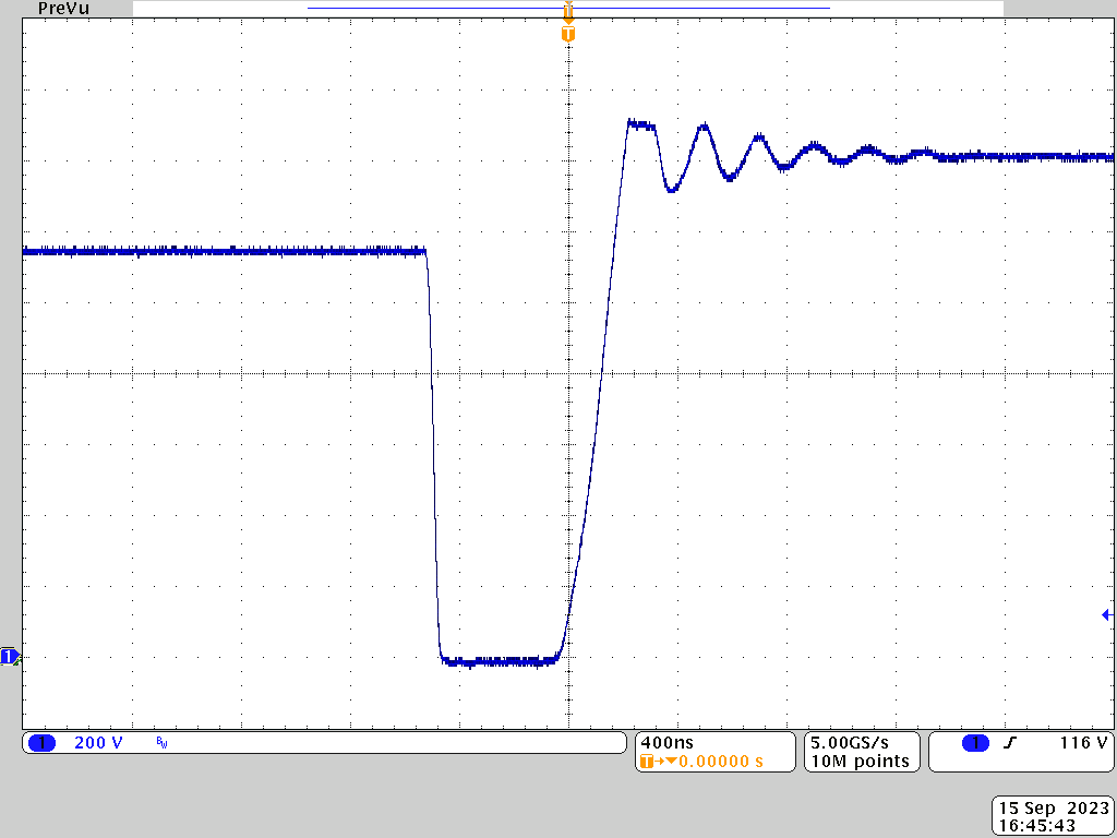 Figure 3-6 VDS of Low-Side
Switch Zoom at
Figure 3-6 VDS of Low-Side
Switch Zoom at1500 VIN, 0-A Load
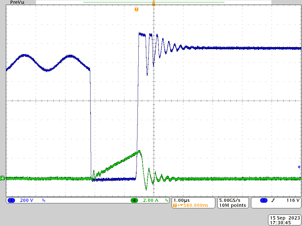
CH1: VDS of
Low-Side Switch Zoom at 1500 VIN, Full Load
CH4: Primary current
Figure 3-8 VDS of Low-Side
Switch Zoom atCH4: Primary current
1500 VIN, Full Load
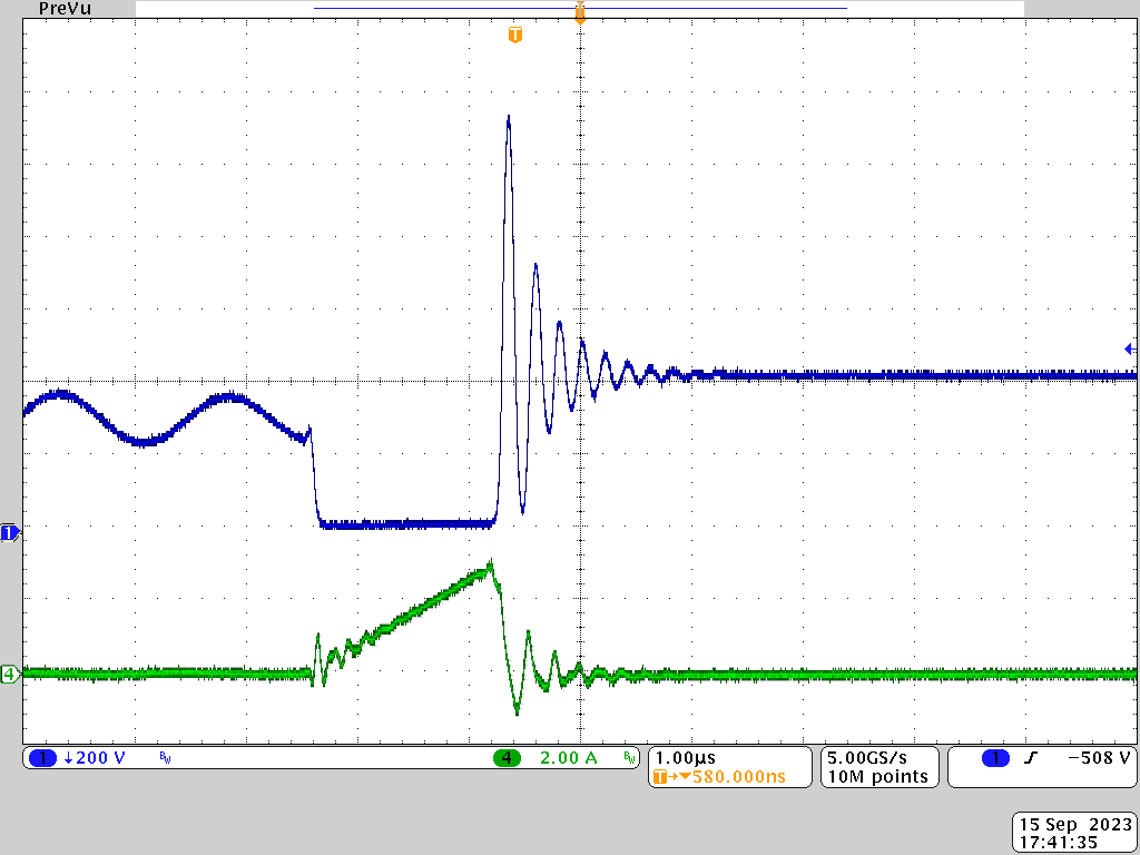
CH1: VDS of
High-Side Switch Zoom at 1500 VIN, Full Load,
CH4: Primary current
Figure 3-10 VDS of
High-Side Switch Zoom atCH4: Primary current
1500 VIN, Full Load