TIDT356
October 2023
1
Description
Features
Applications
1
Test Prerequisites
1.1
Voltage and Current Requirements
1.2
Considerations
1.3
Dimensions
2
Testing and Results
2.1
Thermal Images
2.1.1
10-kHz Switching With 50% Duty Cycle Using the 15-A Gate Drive Output
2.1.1.1
PCB Top Side
2.1.1.2
PCB Bottom Side
2.1.2
10-kHz Switching With 80% Duty Cycle Using the 15-A Gate Drive Output
2.1.2.1
PCB Top Side
2.1.2.2
PCB Bottom Side
3
Waveforms
3.1
Switching
3.1.1
LM5180-Q1 Bias Supply
3.1.1.1
12.4-V Input Voltage – Steady State
3.1.1.2
12.4-V Input Voltage – Gate Drive Transient
3.1.2
UCC5880-Q1 Gate Driver
3.1.2.1
PWM Signal and Gate Drive Signal
3.1.2.2
Gate Drive Turn on
3.1.2.2.1
Comparison (Configurable With External Logic or Through SPI)
3.1.2.2.2
15-A Driver Output
3.1.2.2.3
5-A Driver Output
3.1.2.3
Gate Drive Turn off
3.1.2.3.1
Comparison (configurable with external logic or through SPI)
3.1.2.3.2
15 A Driver Output
3.1.2.3.3
5-A Driver Output
3.2
Load Transients
3.2.1
15-V Output at 12.4-V Input Voltage and 50% Duty Cycle Switching
3.2.2
−8-V Output at 12.4-V Input Voltage and 50% Duty Cycle Switching
3.2.3
15-V Output at 12.4-V Input Voltage and 80% Duty Cycle Switching
3.2.4
−8-V Output at 12.4-V Input Voltage and 80% Duty Cycle Switching
3.3
Start-Up Sequence Isolated Bias Supply LM5180-Q1
3.4
Shutdown Sequence Isolated Bias Supply LM5180-Q1
3.2.2
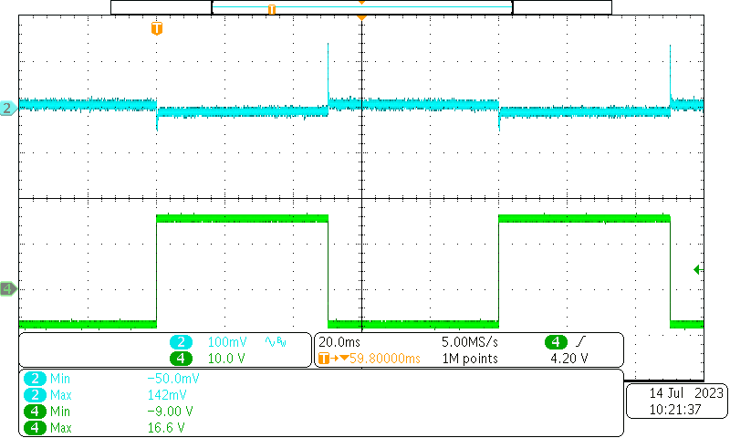
−8-V Output at 12.4-V Input Voltage and 50% Duty Cycle Switching
Ch2: AC-coupled −8-V output voltage, bandwidth limited (20 MHz) [scale: 100 mV / div, 20.0 ms / div]
Ch4: 10-kHz Gate drive switching waveform using the 15-A gate drive output [scale: 10.0 V / div, 20.0 ms / div]
Figure 3-11
Load Transient Behavior of the −8-V Output at 12.4-V Input Voltage and 50% Duty Cycle Switching