TIDT356 October   2023


  1.   1
  2.   Description
  3.   Features
  4.   Applications
  5. 1Test Prerequisites
    1. 1.1 Voltage and Current Requirements
    2. 1.2 Considerations
    3. 1.3 Dimensions
  6. 2Testing and Results
    1. 2.1 Thermal Images
      1. 2.1.1 10-kHz Switching With 50% Duty Cycle Using the 15-A Gate Drive Output
        1. 2.1.1.1 PCB Top Side
        2. 2.1.1.2 PCB Bottom Side
      2. 2.1.2 10-kHz Switching With 80% Duty Cycle Using the 15-A Gate Drive Output
        1. 2.1.2.1 PCB Top Side
        2. 2.1.2.2 PCB Bottom Side
  7. 3Waveforms
    1. 3.1 Switching
      1. 3.1.1 LM5180-Q1 Bias Supply
        1. 3.1.1.1 12.4-V Input Voltage – Steady State
        2. 3.1.1.2 12.4-V Input Voltage – Gate Drive Transient
      2. 3.1.2 UCC5880-Q1 Gate Driver
        1. 3.1.2.1 PWM Signal and Gate Drive Signal
        2. 3.1.2.2 Gate Drive Turn on
          1. 3.1.2.2.1 Comparison (Configurable With External Logic or Through SPI)
          2. 3.1.2.2.2 15-A Driver Output
          3. 3.1.2.2.3 5-A Driver Output
        3. 3.1.2.3 Gate Drive Turn off
          1. 3.1.2.3.1 Comparison (configurable with external logic or through SPI)
          2. 3.1.2.3.2 15 A Driver Output
          3. 3.1.2.3.3 5-A Driver Output
    2. 3.2 Load Transients
      1. 3.2.1 15-V Output at 12.4-V Input Voltage and 50% Duty Cycle Switching
      2. 3.2.2 −8-V Output at 12.4-V Input Voltage and 50% Duty Cycle Switching
      3. 3.2.3 15-V Output at 12.4-V Input Voltage and 80% Duty Cycle Switching
      4. 3.2.4 −8-V Output at 12.4-V Input Voltage and 80% Duty Cycle Switching
    3. 3.3 Start-Up Sequence Isolated Bias Supply LM5180-Q1
    4. 3.4 Shutdown Sequence Isolated Bias Supply LM5180-Q1

PCB Bottom Side

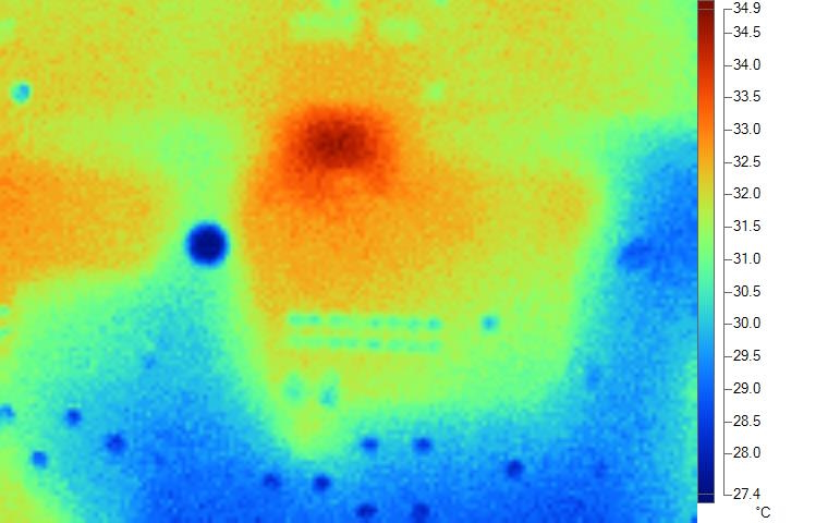
GUID-20230904-SS0I-ZXSN-BXPZ-0WBCZ2DW4445-low.jpg Figure 2-4 PCB Bottom IR Photo for 80% Duty Cycle Switching


On the bottom side of the PCB the area with the largest temperature rise is underneath the IC (U2), where the gate drive signals connect to their respective polygons.