TIDT358 May 2024
3.1 Switching
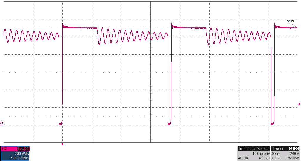
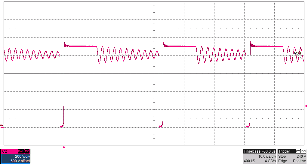
Switching behavior is shown in the following figures.
 Figure 3-1 Switching 1:
800VIN, 33VOUT, 100mAOUT
At 1000VIN, voltage
stress on Q2 is 1150V, the absolute maximum VDS of Q2 is 1200V.
Figure 3-2 Switching 2: 1000VIN, 33VOUT,
100mAOUT