TIDT367 December 2023
- 1
- Description
- Features
- Applications
-
1Test Prerequisites
- 1.1 Voltage and Current Requirements
- 1.2 Required Equipment
- 1.3 Test Setup
- 1.4
Running the Code for Different Labs
- 1.4.1 Lab 1. Primary to Secondary Power Flow, Open Loop Check PWM Driver
- 1.4.2 Lab 2. Primary to Secondary Power Flow, Open Loop CheckPWM Driver and ADC With Protection
- 1.4.3 Lab 3. Primary to Secondary Power Flow, Closed Voltage Loop Check
- 1.4.4 Lab 4. Primary to Secondary Power Flow, Closed Current Loop Check
- 1.4.5 Lab 6. Secondary to Primary Power Flow, Open Loop Check PWM Driver
- 1.4.6 Lab 7. Secondary to Primary Power Flow, Open Loop Check PWM Driver and ADC With Protection
- 1.4.7 Lab 8. Secondary to Primary Power Flow, Closed Voltage Loop Check
- 2Testing and Results
- 3Waveforms
1.3.1 Hardware Setup
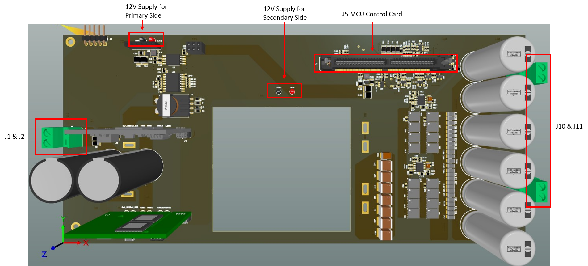
Figure 3-26 shows the board overview for hardware settings.
 Figure 1-1 Board Overview
Use the following procedure when setting up the board:
- Make sure no power source is connected to the board.
- Insert the 280049C controlCARD in the J5 slot.
- Connect a power source for the primary and secondary side (+12 V, 1 A) at the test points
- Switch the power source on for both the primary and secondary side. A green LED on the control card lights up. This indicates the C2000 MCU device is powered.
- To connect JTAG, use a USB cable from the controlCARD and connect the cable to a host computer.
- Connect the DC power supply to the input connector (J1 and J2) and the electrical load to the output connector (J10 and J11).