TIDT369B November   2023  – July 2024


  1.   1
  2.   Description
  3.   Features
  4.   Applications
  5.   Resources
  6. 1System Description
    1. 1.1 System Block Diagram
    2. 1.2 Key System Specification
    3. 1.3 Design Consideration
      1. 1.3.1 Boost Inductor Design
      2. 1.3.2 High Frequency Power Switch Selection
      3. 1.3.3 Input AC Voltage Sensing
      4. 1.3.4 Bulk Voltage Sensing
      5. 1.3.5 Input Current Sensing
      6. 1.3.6 Baby Boost Design
      7. 1.3.7 Relay
      8. 1.3.8 Protection
        1. 1.3.8.1 Over Voltage Protection
        2. 1.3.8.2 Over Current Protection
  7. 2Download Firmware
  8. 3Power Up
    1. 3.1 Required Equipment
    2. 3.2 Considerations
    3. 3.3 Start-Up Sequence
  9. 4Testing Results
    1. 4.1 Start-Up Waveform
    2. 4.2 THD Performance
    3. 4.3 Power Factor
    4. 4.4 Efficiency
      1. 4.4.1 Efficiency Graph
      2. 4.4.2 Efficiency Data
    5. 4.5 E-meter Performance
      1. 4.5.1 E-meter Graphs
      2. 4.5.2 E-meter Data
    6. 4.6 Load Transients
    7. 4.7 Input Current Waveforms
    8. 4.8 AC Drop Test
    9. 4.9 Thermal Images
  10. 5External Reference

Start-Up Sequence

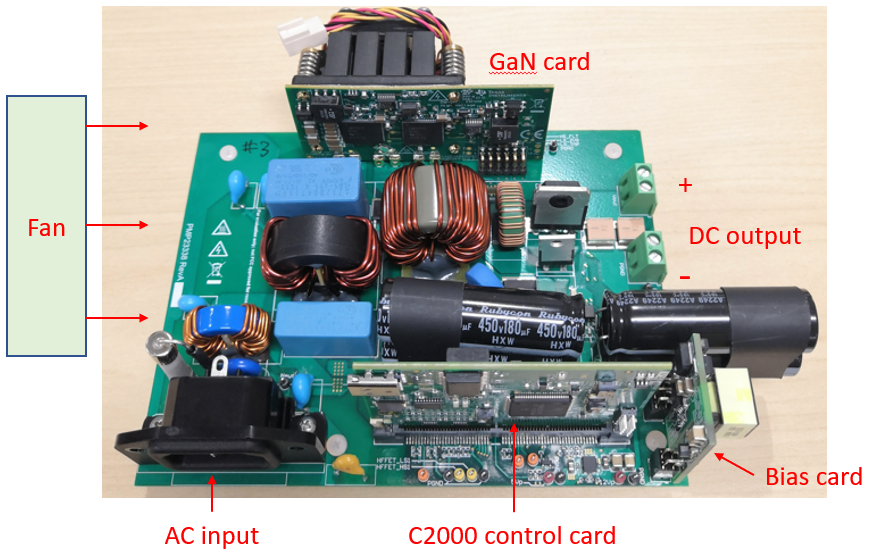
PMP23338 Test setup Figure 3-1 Test setup

Start-up sequence:

  1. Check GaN card, C2000 control card and Bias card are plugged in correctly and tightly
  2. Use a fan for cooling during test
  3. Connect a high voltage load to DC output, set load to 0.1A
  4. Connect AC source to AC input
  5. Use current probe to monitor AC input current, use voltage meter to measure DC output voltage
  6. Set AC output at 115V/60Hz, turn on AC, you see DC output voltage is regulated at about 385V
  7. Graduate increase load. Full load: 1800W@115VAC, 3600W@230VAC