TIDT370 December   2023


  1.   1
  2.   Description
  3.   Features
  4.   Applications
  5. 1Test Prerequisites
    1. 1.1 Voltage and Current Requirements
    2. 1.2 Required Equipment
    3. 1.3 Dimensions
  6. 2Testing and Results
    1. 2.1 Efficiency Graphs
    2. 2.2 Efficiency Data
    3. 2.3 Thermal Images
    4. 2.4 Bode Plots
  7. 3Waveforms
    1. 3.1 Switching
    2. 3.2 Output Voltage Ripple
    3. 3.3 Load Transients
    4. 3.4 Start-Up Sequence

Switching

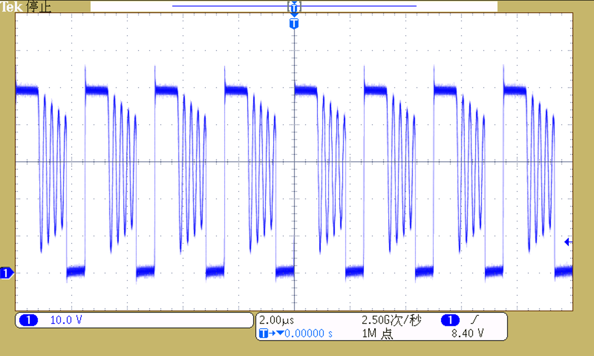
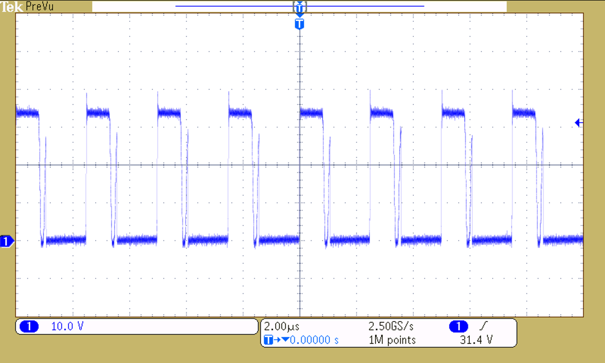
Switching behavior is shown in the following figures.
GUID-20231124-SS0I-BBJK-QFKX-TVQXMJDSBJKK-low.pngFigure 3-1 Switch-Node Voltage, VIN = 13.5 V,
IOUT = 0.5 A
GUID-20231124-SS0I-W111-P7WB-DGLGWCMLT8SD-low.pngFigure 3-2 Switch-node voltage, VIN = 28 V,
IOUT = 0.5 A