TIDT374 March   2024


  1.   1
  2.   Description
  3.   Features
  4.   Applications
  5. 1Test Prerequisites
    1. 1.1 Voltage and Current Requirements
    2. 1.2 Dimensions
  6. 2Testing and Results
    1. 2.1 Efficiency Graphs
    2. 2.2 Thermal Images
      1.      Top Side, 150VAC Input Voltage
      2.      Bottom Side, 150VAC Input Voltage
      3.      Top Side, 254VAC Input Voltage
    3. 2.3 Bode Plot
    4. 2.4 Electromagnetic Interference (EMI) Measurement
  7. 3Waveforms
    1. 3.1 Switching
      1. 3.1.1 150VAC Input Voltage
      2. 3.1.2 254VAC Input Voltage
    2. 3.2 Output Voltage Ripple
      1. 3.2.1 Output 1 (8V)
      2. 3.2.2 Output 2 (18V)
      3. 3.2.3 Output 3 (24V)
    3. 3.3 Input Voltage Ripple
    4. 3.4 Load Transient Output 3 (24V)
    5. 3.5 Start-Up
      1. 3.5.1 150VAC Input Voltage
      2. 3.5.2 253VAC Input Voltage
    6. 3.6 Shutdown
      1. 3.6.1 150VAC Input Voltage
      2. 3.6.2 253VAC Input Voltage

Electromagnetic Interference (EMI) Measurement

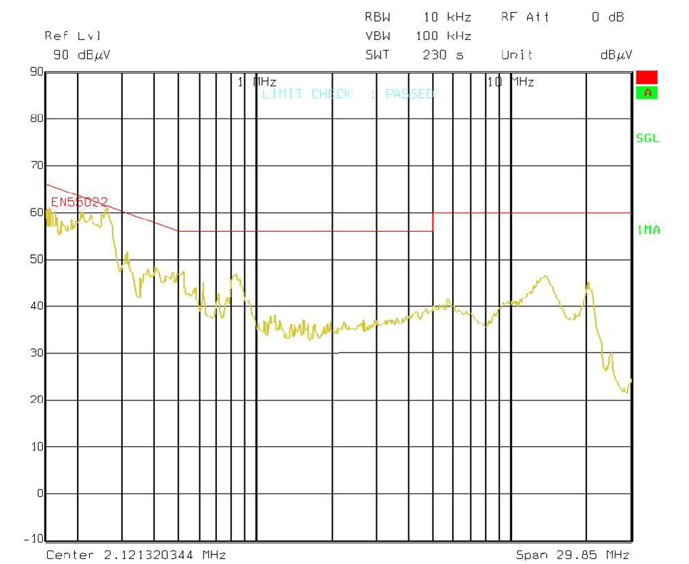
The graph below shows the conducted emission EMI noise and the EN55022 Class-B Quasi-Peak limits (measurement from the worst-case line). The measurement is not certified. The board was connected to a line impedance stabilization network (LISN) and an isolation transformer; the loads were power resistors. The receiver was set to quasi-peak detector, 10kHz bandwidth. The negative terminal of the converter was connected to the ground of the LISN.

Input voltage = 230VAC
Output 1 = 8V at 1A
Output 2 = 18V at 0.25A
Output 3 = 24V at 1.2A
GUID-20240112-SS0I-B5VG-HXKJ-QWVHLBWKSMZZ-low.png Figure 2-7 EMI