TIDT382 February   2024


  1.   1
  2.   Description
  3.   Features
  4.   Applications
  5. 1Test Prerequisites
    1. 1.1 Voltage and Current Requirements
    2. 1.2 Considerations
    3. 1.3 Dimensions
  6. 2Testing and Results
    1. 2.1 Efficiency Graphs
      1. 2.1.1 LM25180-Q1 Efficiency Graph
      2. 2.1.2 SN6507-Q1 Efficiency Graph
      3. 2.1.3 UCC14130-Q1 Efficiency Graph
      4. 2.1.4 UCC25800-Q1 Efficiency Graph
      5. 2.1.5 Efficiency Comparison
    2. 2.2 Efficiency Data
      1. 2.2.1 LM25180-Q1 Efficiency Data
      2. 2.2.2 SN6507-Q1 Efficiency Data
      3. 2.2.3 UCC14130-Q1 Efficiency Data
      4. 2.2.4 UCC25800-Q1 Efficiency Data
    3. 2.3 Load Regulation
      1. 2.3.1 LM25180-Q1 Load Regulation
      2. 2.3.2 SN6507-Q1 Load Regulation
      3. 2.3.3 UCC14130-Q1 Load Regulation
      4. 2.3.4 UCC25800-Q1 Load Regulation
      5. 2.3.5 Load Regulation Comparison
    4. 2.4 Thermal Images
      1. 2.4.1 LM25180-Q1 Thermal Image
      2. 2.4.2 SN6507-Q1 Thermal Image
      3. 2.4.3 UCC14130-Q1 Thermal Image
      4. 2.4.4 UCC25800-Q1 Thermal Image
    5. 2.5 Common-Mode Current (CMI)
      1. 2.5.1 LM25180-Q1 CMI
      2. 2.5.2 SN6507-Q1 CMI
      3. 2.5.3 UCC14130-Q1 CMI
      4. 2.5.4 UCC25800-Q1 CMI
      5. 2.5.5 Common-Mode Current Comparison
  7. 3Waveforms
    1. 3.1 Switching
      1. 3.1.1 LM25180-Q1 Switching
      2. 3.1.2 SN6507-Q1 Switching
      3. 3.1.3 UCC25800-Q1 Switching
    2. 3.2 Output Voltage Ripple
      1. 3.2.1 LM25180-Q1 Output Voltage Ripple
      2. 3.2.2 SN6507-Q1 Output Voltage Ripple
      3. 3.2.3 UCC14130-Q1 Output Voltage Ripple
      4. 3.2.4 UCC25800-Q1 Output Voltage Ripple
      5. 3.2.5 Output Voltage Ripple Comparison
    3. 3.3 Input Voltage Ripple
      1. 3.3.1 LM25180-Q1 Input Voltage Ripple
      2. 3.3.2 SN6507-Q1 Input Voltage Ripple
      3. 3.3.3 UCC14130-Q1 Input Voltage Ripple
      4. 3.3.4 UCC25800-Q1 Input Voltage Ripple
      5. 3.3.5 Input Voltage Ripple Comparison
    4. 3.4 Load Transients
      1. 3.4.1 LM25180-Q1 Load Transients
      2. 3.4.2 SN6507-Q1 Load Transients
      3. 3.4.3 UCC14130-Q1 Load Transients
      4. 3.4.4 UCC25800-Q1 Load Transients
    5. 3.5 Start-Up Sequence
      1. 3.5.1 LM25180-Q1 Start-Up Sequence
      2. 3.5.2 SN6507 Q1 Start Up Sequence
      3. 3.5.3 UCC14130-Q1 Start-Up Sequence
      4. 3.5.4 UCC25800-Q1 Start-Up Sequence
    6. 3.6 Shutdown Sequence
      1. 3.6.1 LM25180-Q1 Shutdown Sequence
      2. 3.6.2 SN6507-Q1 Shutdown Sequence
      3. 3.6.3 UCC14130-Q1 Shutdown Sequence
      4. 3.6.4 UCC25800-Q1 Shutdown Sequence
    7. 3.7 Undervoltage Protection
      1. 3.7.1 LM25180-Q1 Undervoltage Protection
      2. 3.7.2 SN6507-Q1 Undervoltage Protection
      3. 3.7.3 UCC14130-Q1 Undervoltage Protection
      4. 3.7.4 UCC25800-Q1 Undervoltage Protection
  8. 4Summary
  9. 5References

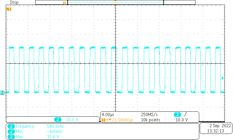
SN6507-Q1 Switching

The SN6507-Q1 switching waveform is shown in the following figure.
GUID-20240116-SS0I-MSWZ-J6DG-TK60NQFLL3BP-low.png
Channel 2: Switching node at 15 VOUT and 100mA load current [scale: 10.0V/div, 4.0μs/div]
Figure 3-2 SN6507-Q1 Switch Node Voltage