TIDT383 March   2024


  1.   1
  2.   Description
  3.   Features
  4.   Applications
  5. 1Test Prerequisites
    1. 1.1 Voltage and Current Requirements
    2. 1.2 Dimensions
  6. 2Testing and Results
    1. 2.1 Efficiency Graphs
    2. 2.2 Efficiency Data
    3. 2.3 Thermal Images
  7. 3Waveforms
    1. 3.1 Switching
    2. 3.2 Output Voltage Ripple
    3. 3.3 Start-Up Sequence

Thermal Images

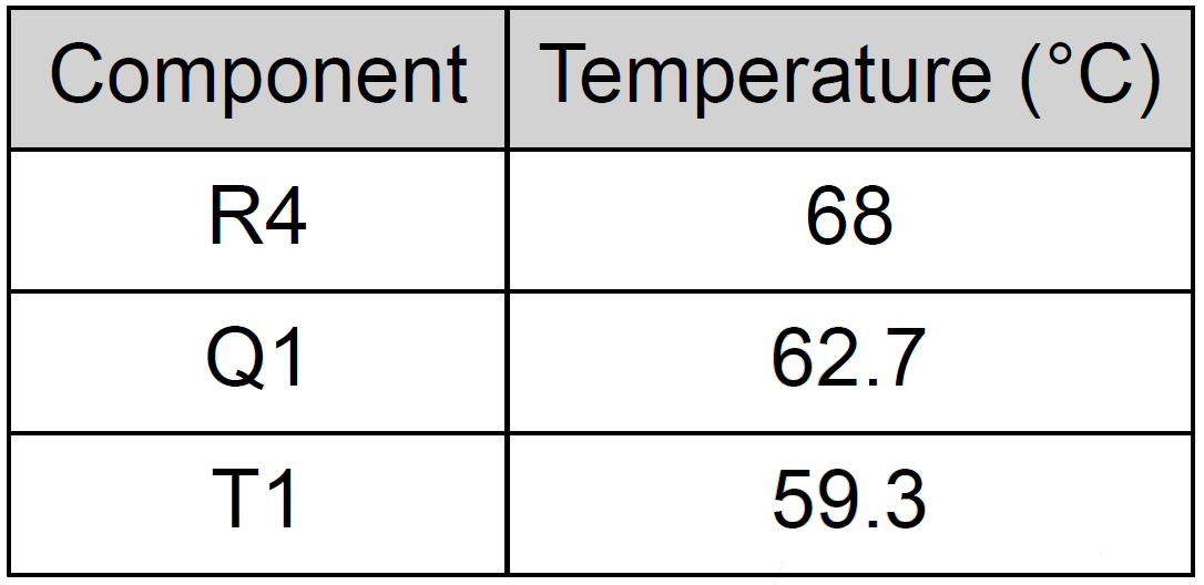
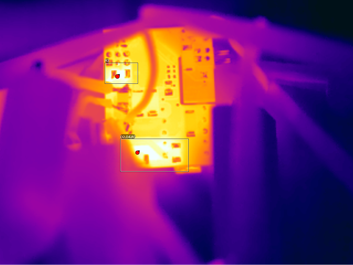
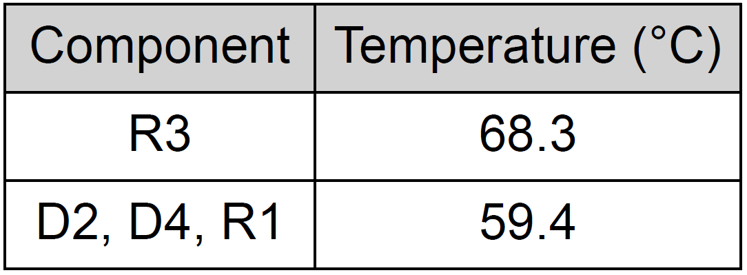
The following thermal images show a top and bottom view of the board. The ambient temperature was 20°C with no forced air flow.

The following conditions apply to these thermal images.

  • 400VDC: PIN = 8.1W, VOUT1 = 12.01V, 0.25A; VOUT2 = 12.45V, 0.0094A;
    VOUT3 = 11.99V, 0.25A; Efficiency = 76%
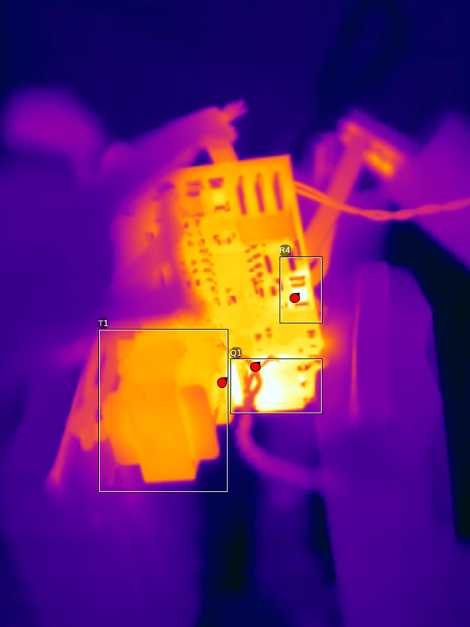
GUID-20240124-SS0I-1RWZ-R4FC-DSW3RQCCB5GR-low.png Figure 2-2 Top Side Thermal Image

GUID-20240207-SS0I-83Z3-PLRL-4W53SJXFVL04-low.png

GUID-20240124-SS0I-F4BT-1Q99-8B6JP98SWTST-low.png Figure 2-3 Bottom Side Thermal Image

GUID-20240207-SS0I-6MRG-6TL3-VBSGVWMMRN2W-low.png