TIDT385 May 2024
3.1 Switching Waveforms
Switching behavior is shown in the following figures.

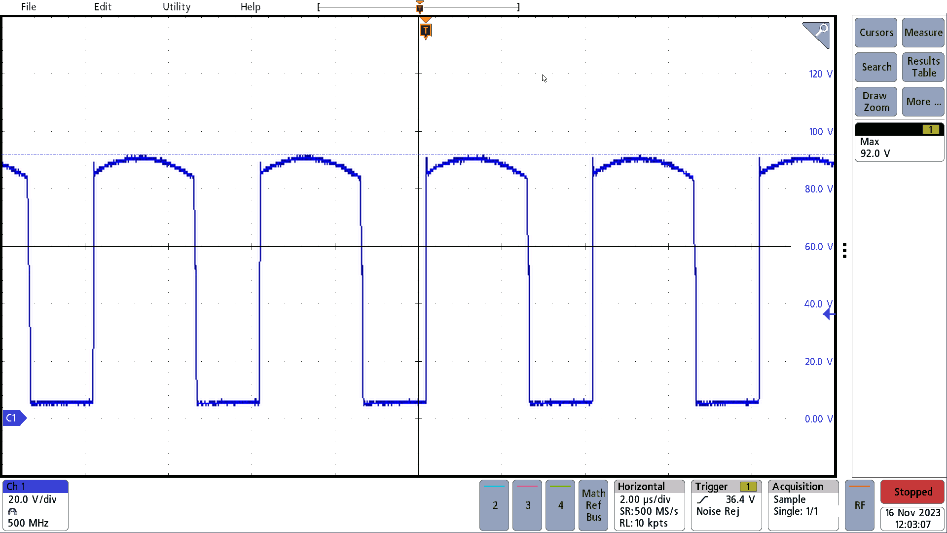
57VDC input, 20V / div, 2μs / div,
measured 92.0V peak
Figure 3-1 Primary FET Q27, Drain to PGND
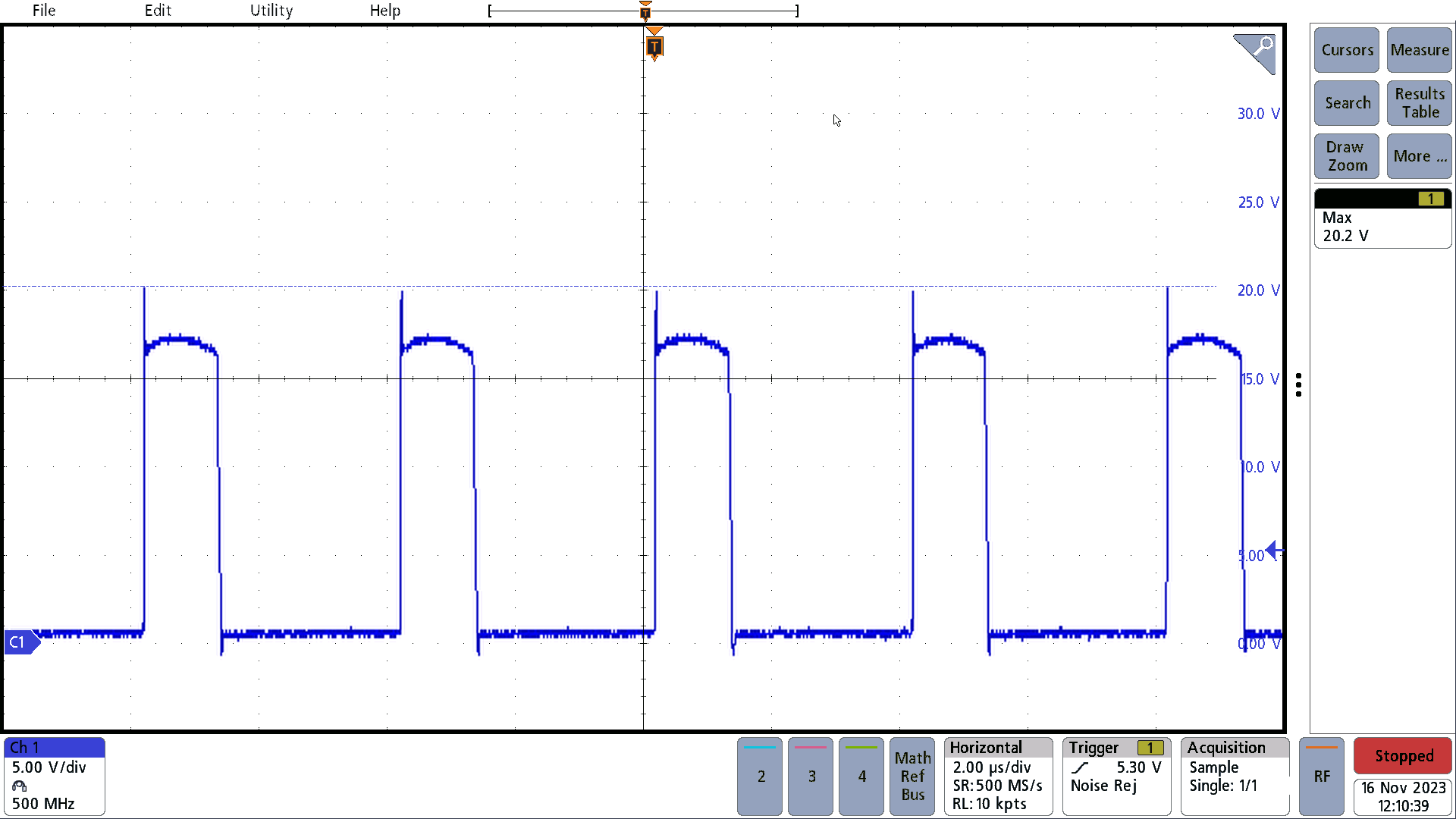
32VDC input, 5V / div, 2μs / div,
measured 20.2V peak
Figure 3-2 Secondary Synchronous FET Q28, Drain to
GND
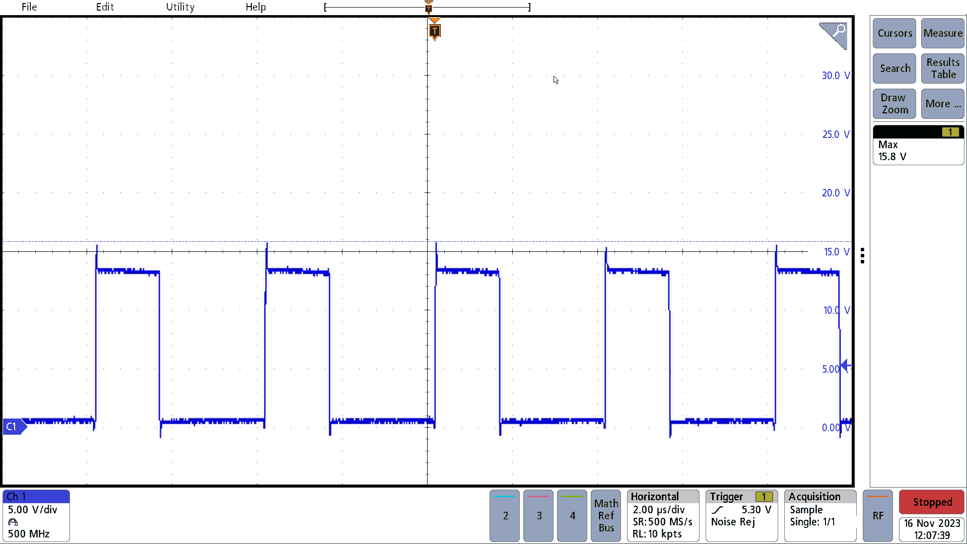
57VDC input, 5V / div, 2μs / div,
measured 15.8V peak
Figure 3-3 Secondary Synchronous FET Q25, Drain to GND