TIDT396 June   2024


  1.   1
  2.   Description
  3.   Features
  4.   Applications
  5. 1Test Prerequisites
    1. 1.1 Voltage and Current Requirements
    2. 1.2 Required Equipment
    3. 1.3 Considerations
    4. 1.4 Dimensions
  6. 2Testing and Results
    1. 2.1 Efficiency Graph
    2. 2.2 Efficiency Data
    3. 2.3 Thermal Image
    4. 2.4 Bode Plots
  7. 3Waveforms
    1. 3.1 Switching
    2. 3.2 Voltage Ripple
    3. 3.3 Load Transients
    4. 3.4 Turn-on Response

Switching

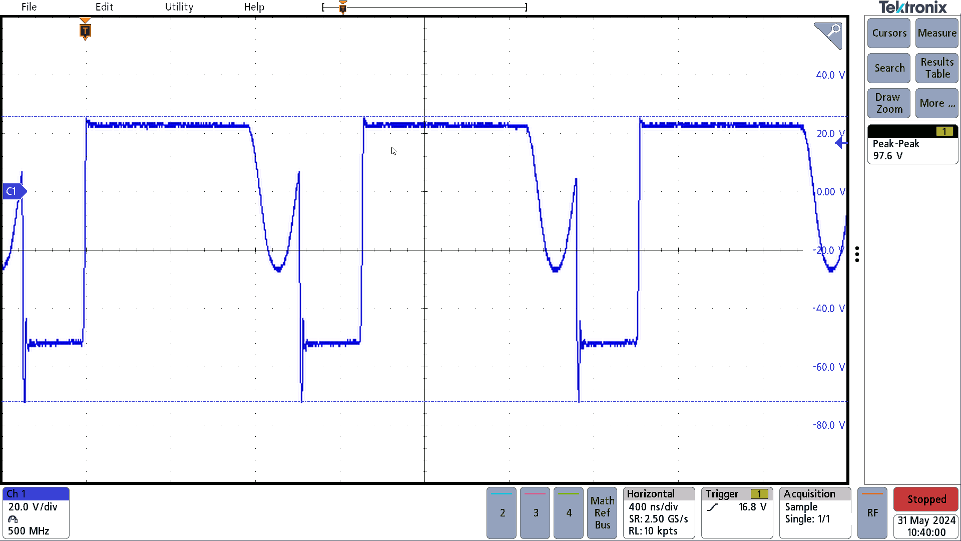
PMP23470 Diode D2 Voltage Figure 3-1 Diode D2 Voltage

Anode to GND voltage, 57V input

20V/div; 400ns/div; 500MHz bandwidth

Measured 97.6Vpeak-to-peak
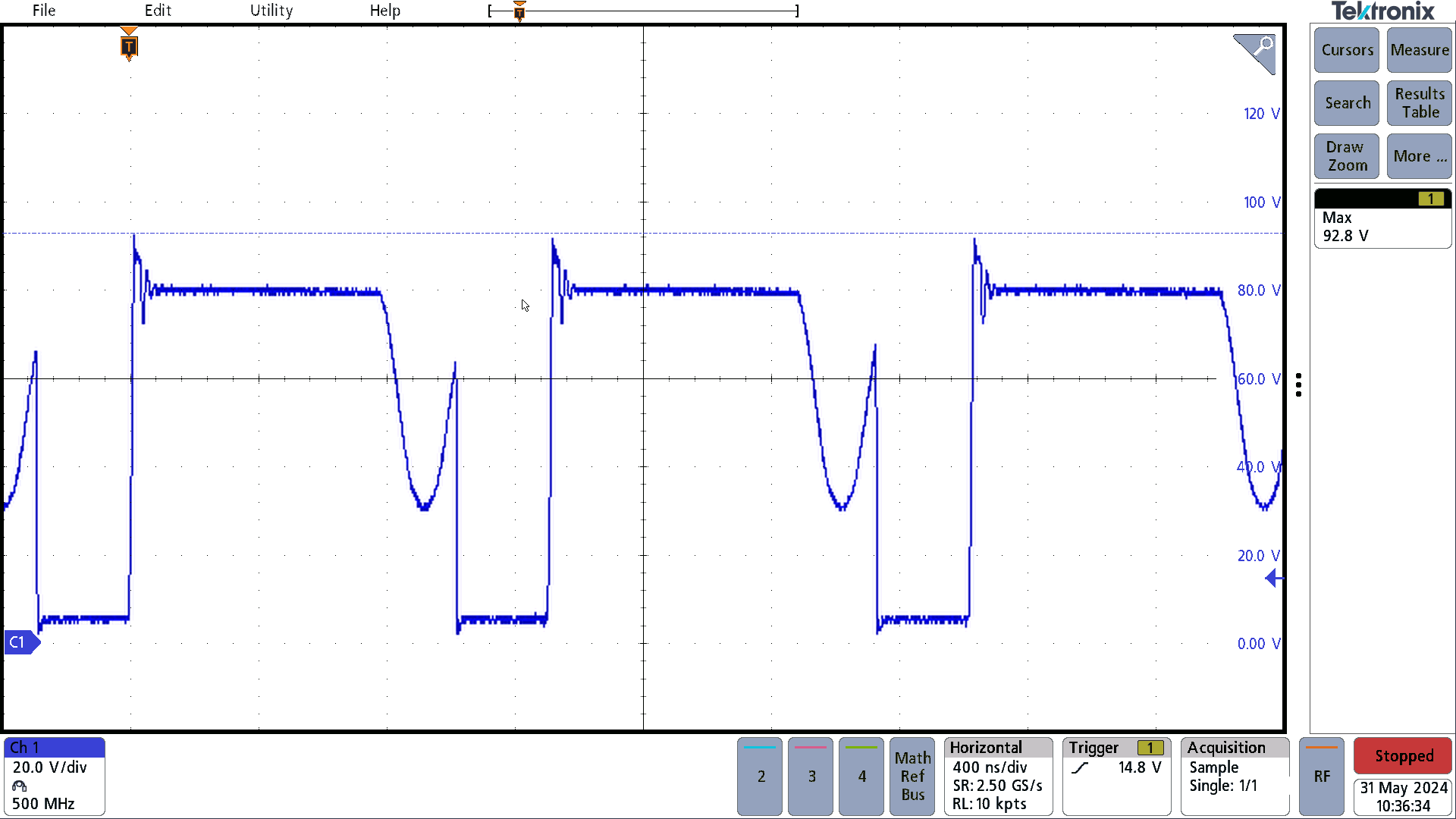
PMP23470 MOSFET Q2 VoltageFigure 3-2 MOSFET Q2 Voltage

Drain to PGND voltage, 57V input

20V/div; 400ns/div; 500MHz bandwidth

Measured 92.8Vpeak